Silicon based SPADs have demonstrated superior performance and thanks to this, they found place in various applications, such as fluorescence lifetime imaging (FLIM), positron emission tomography (PET) and time-of-flight laser ranging (LiDAR). However, they suffer from low detection efficiency in short-wave infrared due to silicon bandgap and this prevents them from being used in applications like eye-safe time-of-flight laser ranging or quantum key distribution. Since this problem occurs due to an intrinsic property of silicon, the light absorbing material of the SPAD has to be replaced with materials that have a smaller bandgap.
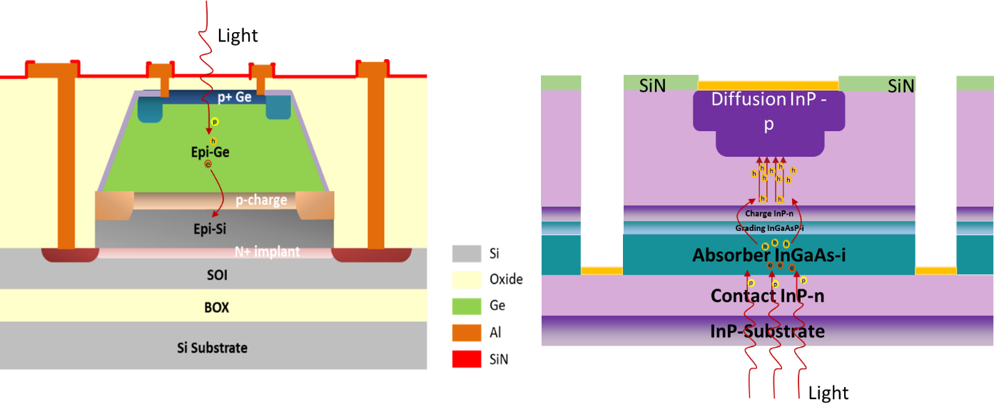
In this sense, Germanium and InGaAs materials are two promising candidates to achieve high performance operation at infrared regime with almost 1.6 and 1.7 μm cutoff wavelengths at room temperature. We are currently designing and fabricating devices based on the utilization of both. The very first challenge of working with narrow bandgap materials is that when they are exposed to high electric field to induce impact ionization, band-to-band tunneling becomes severe. This results in a very poor noise performance. Therefore, unlike silicon based SPADs, in which the devices are just p-n junctions, Germanium and InGaAs based SPADs have an advanced junction structure, called separate absorber, charge and multiplication type. The main idea of such a structure is to have absorption in the narrow bandgap material and impact ionization (multiplication) in the high bandgap material. In order to implement such a device, one has to consider the lattice matching conditions of InGaAs and Germanium to a high bandgap material. InP for InGaAs and Silicon for Germanium are common solutions to be used as multiplication material. Germanium on Silicon has a capability of being CMOS compatible so that it is possible to easily integrate the read-out electronics with the SPAD on the same chip, but it suffers from slight lattice mismatch and low absorption coefficient. InP and InGaAs are perfectly lattice matched to each other at 0.53 In mole fraction and InGaAs has a very high absorption coefficient. However, in order to integrate them with electronic circuits, chip to chip bonding is required which is a more expensive approach compared to the former one. In our research, we are exploring both options and trying to optimize device designs for the best performance [1].
Relevant Publications
- Sammak, A., Aminian, M., Qi, L., de Boer, W. B., Charbon, E., & Nanver, L. K. (2011, December), “A CMOS compatible Ge-on-Si APD operating in proportional and Geiger modes at infrared wavelengths”, in 2011 International Electron Devices Meeting (pp. 8-5), IEEE.