MEMS-Based Zero-Power Reconfigurable PICs
Our group participates in the H2020 collaborative project for the design and manufacturing of MEMS Based Zero-Power Reconfigurable Photonic Integrated Circuits. We are pleased to contribute to the project with our expertise in the design of Silicon Photonic MEMS components and large scale circuits, and lead the development of the MEMS related fabrication processes.
The complexity of photonic integrated circuits (PIC) has steadily increased over the past decade. PICs combine many optical functions (wavelength filtering, modulation, photodetection) on a chip. Just like in electronic integrated circuits (IC), the functionality of a complex photonic circuit is as much determined by the number and the connectivity of its elements than by the performance of the individual building blocks. Silicon photonics is the only photonic integration technology that can support the required component density needed for a sustained scaling of complexity in photonic integrated circuits. This is enabled by the high refractive index contrast and the compatibility with high-end CMOS manufacturing processes. The high contrast between silicon and its oxide (SiO2) makes it possible to confine infrared light into a sub-micrometer optical waveguide and bend light with a < 5 μm radius. Silicon photonic circuits are usually implemented on silicon on insulator (SOI), which is compatible with the fabrication processes used for CMOS electronics. This makes it possible to leverage an established high-volume manufacturing base. Because of these assets, silicon photonics research has grown exponentially over the past decade and is now experiencing industrial adoption with first products on the market. Today, this development is largely driven by datacentre communications and telecom, but silicon photonics is also proving its capabilities in (bio)sensor, microwave and spectroscopy applications.
Even with this rapid evolution, today’s silicon photonics technology suffers from two limitations that constrain the scaling of circuits:
- Variability: the high contrast of SOI makes the components extremely sensitive to nanometre-scale variations. Because of this, even the best processes are limited in the number of components in a circuit without suffering from mismatched response due to stochastic variations.
- Power consumption: while variations can be compensated by active tuning, the current technique of thermal tuning draws too much power to accommodate many tuning elements.
MORPHIC addresses these limitations by introducing micro-electro-mechanical systems (MEMS) into silicon photonic circuits. Photonic MEMS actuators provide the strongest possible electro-optic effect in on-chip technology, because they induce a physical change in the material distribution. Moreover, as MEMS work through electrostatic force, they have a very low power consumption. By adding mechanical latching mechanisms, MEMS become non-volatile, i.e. they maintain their state without power.
We will enhance an established Silicon Photonics platform with MEMS actuators so photonic circuits can be programmed, and reprogrammed, for a variety of optical functions with built-in redundancy and resilience. To achieve that, MORPHIC will introduce:
- Low-power photonic MEMS actuators into silicon photonics,
- Non-volatile mechanical latching operation,
- Programmable connectivity implemented in a large-scale circuit matrix.
Here at EPFL, we perform the mechanical design and simulation of the MEMS devices using finite element method software, such as COMSOL, and do the same in the optical domain with finite-difference time-domain software, such as Lumerical. Designs conform to the specifications of IMEC’s iSiPP50G technology, an established silicon photonics platform and make use of the high performance passive and active components already provided as part of the library of standard components (e.g., ultra-low loss waveguides, high efficiency grating couplers, and high-speed modulators and detectors).
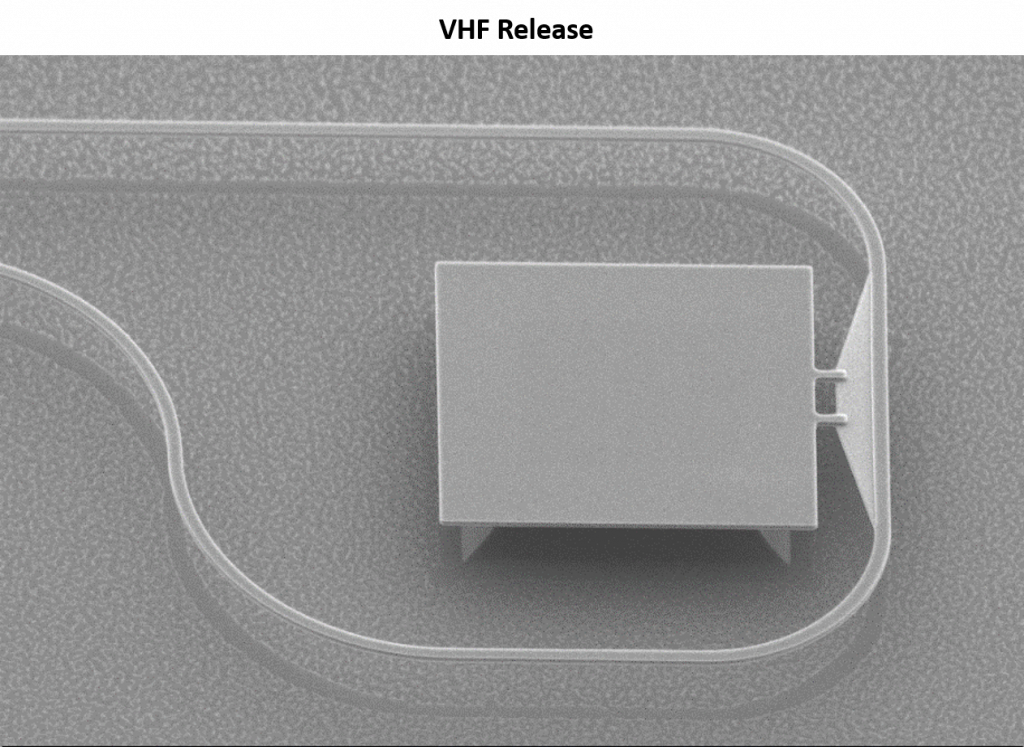
After fabrication at IMEC, samples are delivered to EPFL where they undergo a post-processing sequence to “release” the MEMS device and make them free-standing and movable. Fabrication steps include an alumina passivation to protect regions of the chip that should not be etched by the vapor phase HF (VHF) that removes the sacrificial oxide under the MEMS device, a lithography step, and two etching steps, one to open up windows in the passivation, and the final VHF etch.
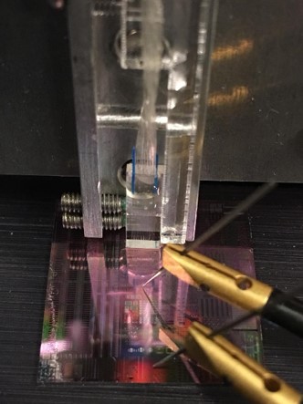
Characterization is carried out in the Q-lab laboratory using a tunable laser with photodetectors, a fiber array, and electrical probe tips attached to micropositioners to provide the actuation voltage for the MEMS devices.
Funding and Management
The MORPHIC project has received funding from the European Union’s Horizon 2020 research and innovation programme under grant agreement No 780283.
Project Start : January 2018.
Duration : 3.5 years.
More information on the project can be found on the dedicated project website https://h2020morphic.eu/.
