2D-Materials for Bolometers of the Future
label0=
2D Material Based Bolometers
Remote thermal sensing and imaging is currently one of the most prominent technological fields. It is raising a lot of industrial interest as its market value is expected to grow beyond $10 billion/year by 2020. The simplicity and low price of uncooled radiation heat sensors, bolometers, have made them subjected for extensive research. The route for improved performance is enhanced absorption of thermal radiation, improved thermal isolation, reduced thermal mass, increased sensitivity of thermal transduction and reduced noise. However, even though the route is clear, bolometer technology has stagnated over the last decade.
FUTBOL aims to cause a paradigm shift in bolometer technology by making use of suspended devices made of 2D materials to create a novel sensor with unseen resolution and bandwidth. Indeed, atomically thin crystalline materials, 2D materials, are an attractive alternative to traditional bolometer materials. Their extreme aspect ratio allows for excellent thermal isolation, low areal mass density results in a microscopic thermal mass. Electrostatically tunable electrical and optical properties enable strong light-matter interaction.
The Concept
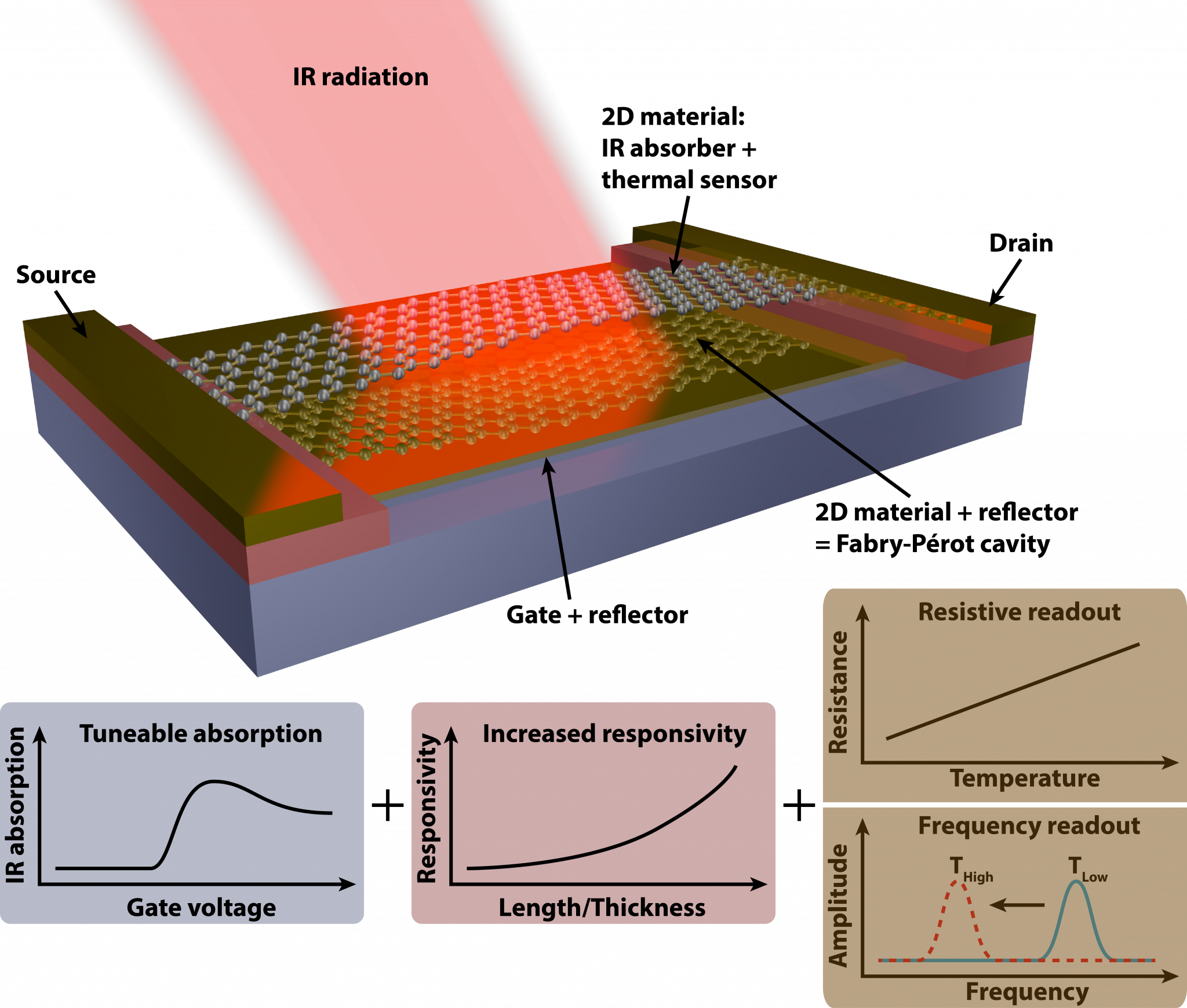
The figure below shows a schematic of the 2D material based bolometer. A strip of 2D material is suspended to thermally isolate it from its surroundings and form a Fabry-Pérot cavity. Thermal radiation is partly absorbed and partly transmitted into the cavity where it resonates between a reflector and the 2D material. As the 2D material is not a perfect mirror it will eventually absorb a large fraction of the radiation. The conductivity of the 2D material is electrostatically tuned, using the gate voltage, to maximize absorption. It is utilized that an ultrathin metallic layer reaches 100% absorption when its resistance equals the product of the layer thickness times the vacuum impedance. Absorption of radiation leads to heating of the thermally self-sensing 2D material which is transduced either via changes in its electrical resistance (traditional readout) or mechanical resonance frequency. Advantages of the bolometer design are minimal thermal mass, excellent thermal isolation, short time constant and the ability to electrostatically tune the absorption of radiation, combined leading to unseen resolution and bandwidth.
Fabrication
For the fabrication of graphene based mechanical resonators, we worked on two approaches in parallel. (i) Graphene membranes resonators – no electrodes and (ii) clamped-clamped graphene beam resonators suspended above a gate electrode and contacted by source and drain electrodes. The first approach is the simplest one and the chance of success is higher. However, electrical transduction of the membranes is not possible and optical detection has to be used instead. The second approach allows electrical transduction but the fabrication process is more complex.
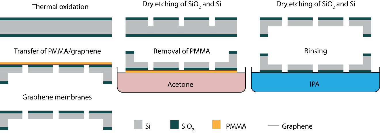
The figure below shows a schematic of the fabrication process used to realize graphene membranes. Holes defining the size of the membranes are etched into the front side of a silicon wafer with 300 nm of thermal oxide. Large openings are etched into the backside of the wafer until they meet the front side etched holes to create through wafer holes. Through holes are needed to avoid trapping water in the holes when transferring graphene onto the chip. A PMMA/graphene thin film is transferred onto the front side of a chip to form PMMA/graphene membranes. The PMMA is removed in acetone. Finally the chip is rinsed in isopropanol. Only the front side of the chip is exposed to acetone and isopropanol. Otherwise liquid trapped in the holes will lead to collapse of the membranes when drying due to capillary forces.
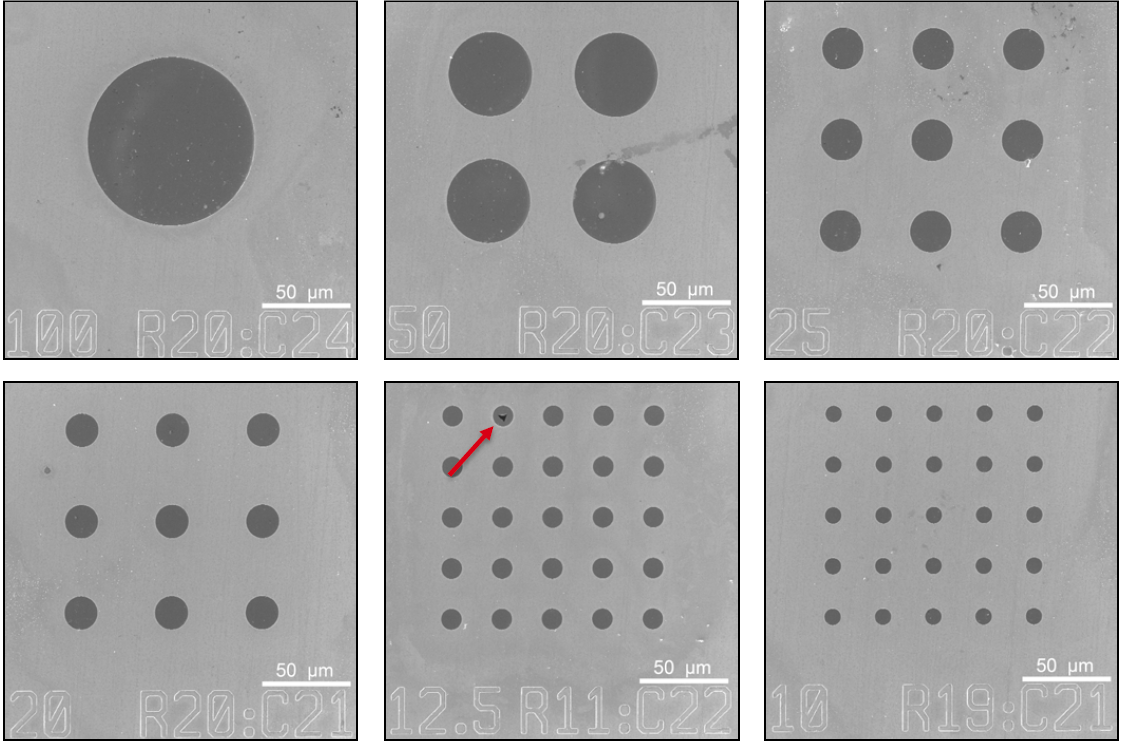
The figure below shows a collection of fabricated graphene membranes ranging in diameter from 10 µm to 100 µm. The diameter to thickness ratio of these membranes ranges from 30,000-300,000. A sample with a broken membrane, marked with red arrow, is included in the collection. This allows one to see the difference between intact and broken membranes. Using the above mentioned fabrication method membranes of this type can fabricated with a high yield.
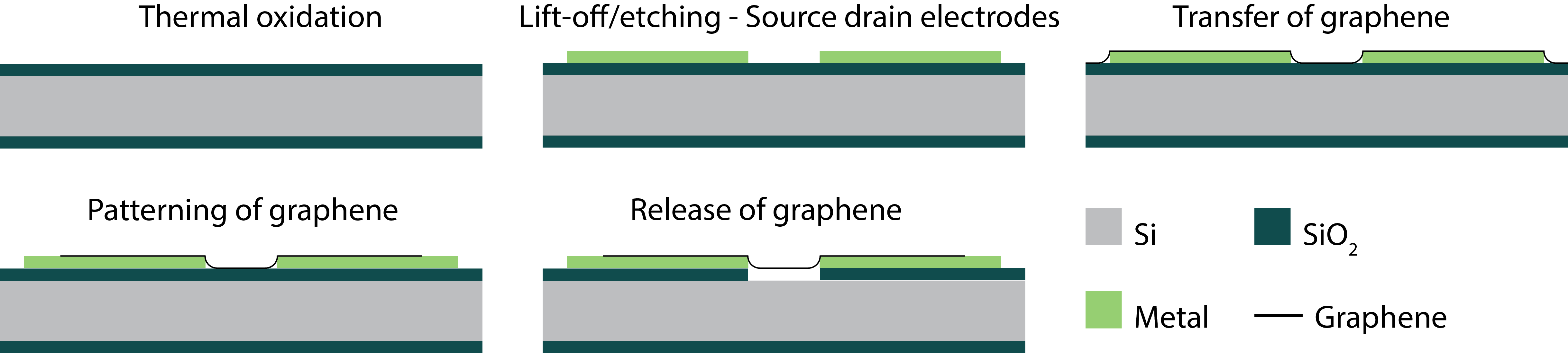
The figure below shows a schematic of the fabrication process used to realize suspended sheets of graphene place above a gate electrode and contacted by source and drain electrodes. This fabrication process minimizes post transfer processing, which is known to affect the electrical properties of graphene. The fabrication process is as follows: (i) 300 nm thick silicon oxide is grown on a highly doped silicon wafer. (ii) source and drain electrodes are defined using lift-off. (iii) CVD graphene is transferred onto the chip; and (iv) patterned using dry etching. The graphene is released by etching the supporting oxide. To avoid stiction, critical point drying is used.
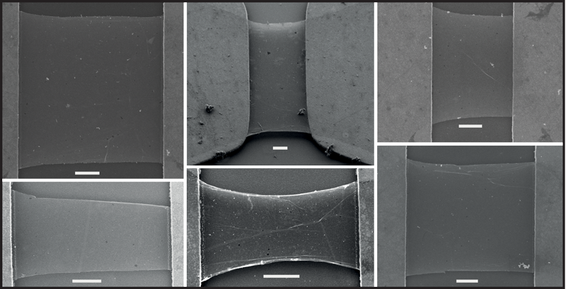
The figure below shows a collection of released clamped-clamped graphene beams. Beams ranging in width and length from 3-8 µm and 2-8 µm, respectively, were successfully fabricated. The scale bars in the picture are all 1 µm.
Characterization
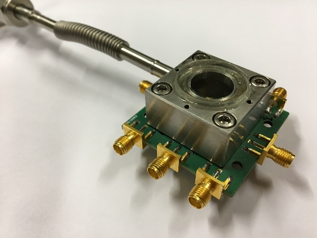
Characterization of devices is primarily done in vacuum. To secure fast pump down time we use a vacuum solution where the vacuum chamber is mounted directly on top of the PCB containing the wire-bonded chip, see figure below.
Electrical Characterization
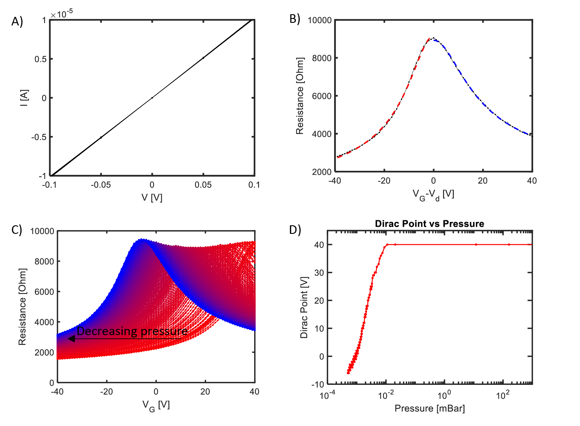
The figure below shows the electrical characterization of unsuspended graphene devices. (A) shows 50x current-voltage curve for a single device. The characteristic is highly linear and drift/aging is negligible. (B) shows the source-drain current as a function of the gate voltage around the Dirac point. By sweeping the gate voltage we are able to modulate the resistance by more than 300%. The dashed lines in the plot are fits from which we can extract the charge carrier mobility in the graphene, ~750 cm/V/s for both holes and electrons. (C) shows a series of gate sweep plots. The sweeps are taken one after another while evacuating the vacuum chamber. The gate voltage for the Dirac point is decreasing for decreasing pressure. A process that is reversible when venting the chamber. Charge carrier mobility’s stay constant despite the large change in the gate sweep curves. (D) show the Dirac point as a function of pressure. The movement of the Dirac point is believed to be associated with the desportion/adsorption of water molecules on the graphene.
Mechanical Characterization
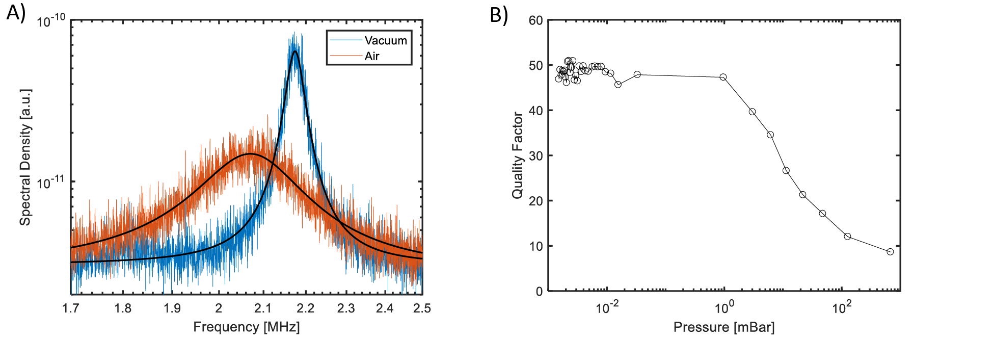
The figure below (A) shows the resonance frequency, measured by laser Doppler vibrometry, of a 20 µm diameter graphene membrane in air and vacuum. (B) shows the quality factor as a function of pressure. The transition from intrinsic to viscous damping takes place between 1 and 100 mBar.
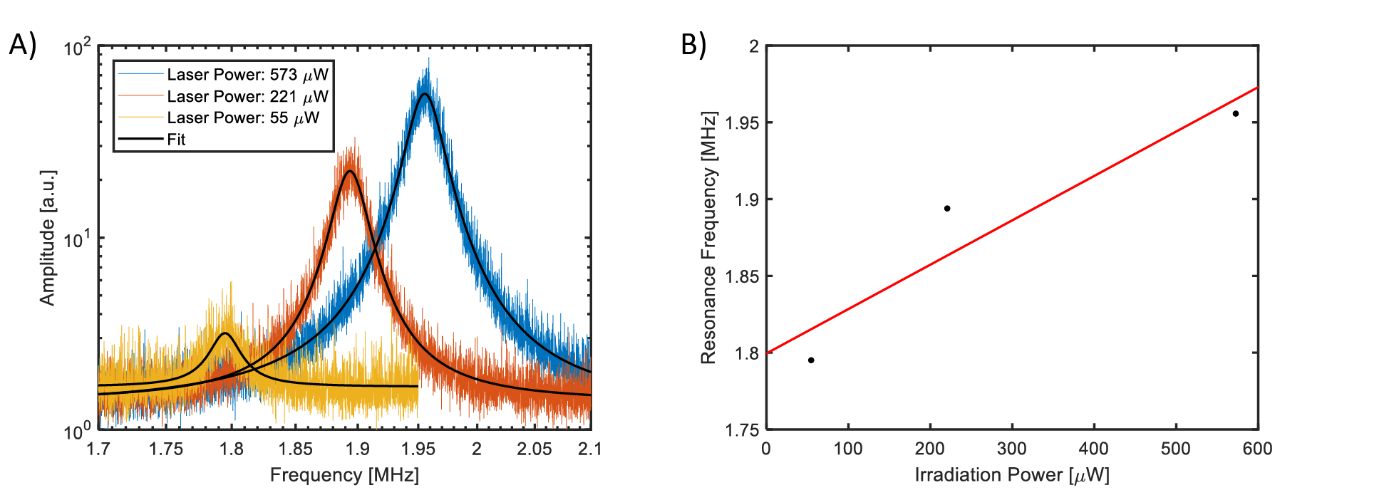
Change in frequency per absorbed power of a graphene membrane was measured by varying the power of the optical readout laser. (A) below shows the measured frequency spectrum for three different level of radiation. (B) shows the resonance frequency as a function of irradiation power. The resonance frequency is increasing as a function of irradiation power. This trend is opposite to what would be seen for e.g. a silicon or silicon nitride resonator. This behavior can be explained by the negative thermal expansion coefficient of graphene. The relative change in frequency per irradiation power is 0.016 %/µW. Graphene is know to have an absorption coefficient of 2.3%. Taking this into account the effective responsivity is estimated to 0.71%/µW.