Our research activities focus on the study and development of NEMS/MEMS resonators. We target two main applications: sensors and communications. We follow a holistic approach so we have projects/ideas on analysis, modelling, fabrication, characterization, integration, and application of these devices.
Below you can find a list with some ideas for semester and master projects. Do not hesitate to contact us because we will likely be able to find a project that matches your motivations.
Pour les étudiants francophones, s’il vous plaît ne pas hésiter à nous contacter, car nous pouvons également parler en français.
ANEMS project on ISA (Beta)
Collaborations with companies
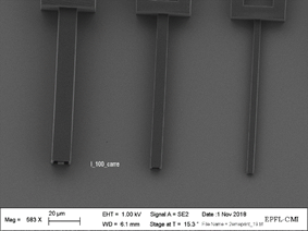
The projectVibration sensors (aka vibrometers) are essential components to keep safety and reliability of different types of machines, e.g. plane engines. A vibrometer is able to detect very small vibrations, that coming from either acceleration caused at the clamp or by pressure variations in the environment. In the frame of aerospace industry, the extremely strict requirements for safety, resolution, endurance and lifetime have caused the technology to evolve very slowly. The idea of the project is to analyze if a MEMS based device would be of interest as the next generation vibrometers. Analysis of the different transduction possibilities, design and fabrication in the CMi clean room at EPFL will be performed. The CompanyMeggitt Sensing Systems Switzerland (MSS Switzerland) leads the market in sensing and monitoring solutions, specialising in smart engineering for extreme environments. Our 60+ years of sensor and system expertise means our solutions are trusted by original equipment manufacturers around the world. MSS Switzerland was founded as Vibro-Meter® back in 1952. This became a Meggitt company in 1998 and in 2006 was integrated in the Meggitt Sensing Systems division.
Project Components:The project will be carried at the Advanced NEMS group at EPFL (Lausanne), but with often visits to the Meggit-sensing site in Fribourg. The main tasks involved in the project will be:
Desired Skills:
|
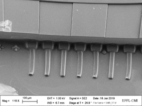
The projectThe availability of suitable sensors becomes increasingly challenging in harsh environments , typical of many industrial settings, where e.g. high temperatures, high pressures, large electromagnetic fields or radiation hinder the use of conventional electronic transducers. Optical-based sensors provide a route towards circumventing these difficulties. In particular, micro-optomechanical systems (MOMS) combining a mechanical element with optical readout techniques can be fabricated to tolerate harsh conditions. The ability to build them into optical fibers provides ease of scalability, distribution and installation in systems requiring multiple sensors, and their integration into available optical communication networks. The project aims at designing and fabricating micro-mechanical devices and resonators to be assembled in the final product with optical readout. There will be the opportunity to participate in the overall prototypes and products development, interact with external suppliers and clients (in defense, energy, automotive, aerospace), learn new challenging techniques and discover the tech startups world. The master project will be sponsored. Possibility to join the startup after the project. The companyThe Miraex is a young startup based at the EPFL Innovation Park. Miraex unique combination of nanotechnoly, new materials, photonics and artificial intelligence provides the missing tool for predictive maintenance in harsh environments. By harnessing the power of light, Miraex products enable smarter and greener factories for the Industry 4.0 Possibility to join the startup after the project.
Fig. 1 Micro-optomechanical systems (MOMS) before integration in the prototype Project Components:The project will be carried out between Miraex (EPFL Innovation Park) and the Advanced NEMS group at EPFL (Lausanne). The main tasks involved in the project will be:
Desired Skills:
|
 |
Semester/Master Project |
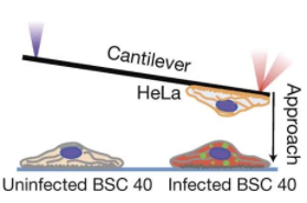
The project
In collaboration with Nanosurf we would like to develop a new generation of cantilevers that are compatible with AFM holders and measurement setup, so that they provide a much more reliable measurement for cell growth.
Nanosurf was founded in 1997 in Liestal, Switzerland, and has since become one of the most trusted and established AFM brands in the market today. Nanosurf has a vast knowledge base in scanning probe microscopy, with an average of more than 15 years of AFM experience in our sales, service and development teams.
In this project we will design, simulate, fabricate and characterize a novel type of cantilever that is compatible with Nanosurf equipment and that allows a more stable measurement for cell growth. We will adapt the load depending whether you are a semester or a master student.
|
 |
|
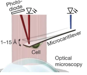
Fig. 1: Schematic of the detection scheme of the AFM |
Fig.2: Cell interaction with AFM |
Project components
- Design, simulation, fabrication
Desired skills
- Comsol, Fab experience would be welcome
|
Type of Project: Section(s): Contact(s): |
Semester/Master Project Electrical and Microengineering; Mechanical Engineering; |
Semester (or Master) project
The project
Crystalline SiO2, known as quartz, is one of the most successful examples of a piezoelectric material employed in miniaturized time reference circuits, thanks to its high quality factor and low temperature dependency.
One of the main drawbacks of quartz is the limited piezoelectric coefficient which impacts the energy conversion efficiency between electrical and mechanical domains. The objective of this project is to couple quartz with thin film piezoelectric materials such as Aluminum Nitride which show a larger piezoelectric coefficient, to benefit from the strong points of each material.
The project objective is to develop a protocol to deposit high quality films on quartz with reactive sputtering. Future developments would be patterning of test devices as a demonstration.
The company
Micro Crystal AG, a company of the Swatch Group Inc. Switzerland, founded in 1978, is a leading manufacturer of Miniature Quartz Crystals (32kHz to 250MHz), Real Time Clocks, Oscillators and OCXOs for the world’s leading manufacturers of Wearables, IoT, mobile phones, consumer products, computers, automobile electronics, watches, industrial controls, as well as medical implantable devices and other high-reliability product applications. With offices located around the globe, Micro Crystal AG provides in-depth support for our customers from design-in to mass production.
References:
[1] J. Liang, J. Huang, T. Zhang, J. Zhang, X. Li, and T. Ueda, “An Experimental Study on Fabricating an Inverted Mesa-Type Quartz Crystal Resonator Using a Cheap Wet Etching Process,” Sensors, vol. 13, no. 9, Art. no. 9, Sep. 2013, doi: 10.3390/s130912140.
[2] P. Kunicki, M. Moczała-Dusanowska, G. Jóźwiak, P. Szymanowska, T. Piasecki, and T. Gotszalk, “Quartz tuning fork mass change sensing for FIB/SEM technology,” Micron, vol. 129, p. 102792, Feb. 2020, doi: 10.1016/j.micron.2019.102792.
|
|
|
|
Fig. 1: Inverted-mesa type Quartz resonator [1] |
Fig.2 : Tuning Fork type quartz resonator [2] |
Project components
- Develop a recipe for deposition of AlN on quartz, included a clamping holder to adapt to multiple substrate sizes
- Characterize film growth with SEM, XRD and stress measurements
Desired skills
- Previous cleanroom experience appreciated but not necessary
- Microfabrication technology (especially Physical Vapor Deposition) knowledge
References:
[1] J. Liang, J. Huang, T. Zhang, J. Zhang, X. Li, and T. Ueda, “An Experimental Study on Fabricating an Inverted Mesa-Type Quartz Crystal Resonator Using a Cheap Wet Etching Process,” Sensors, vol. 13, no. 9, Art. no. 9, Sep. 2013, doi: 10.3390/s130912140.
[2] P. Kunicki, M. Moczała-Dusanowska, G. Jóźwiak, P. Szymanowska, T. Piasecki, and T. Gotszalk, “Quartz tuning fork mass change sensing for FIB/SEM technology,” Micron, vol. 129, p. 102792, Feb. 2020, doi: 10.1016/j.micron.2019.102792.
|
Type of Project: Section(s): Contact(s): |
Semester/Master Project IEM, IGM, ISIC |
Resonators with Microchannels
 |
Master Project You will mostly do Design and Fabrication We want to analyze biosamples via acoustic waves |
The project
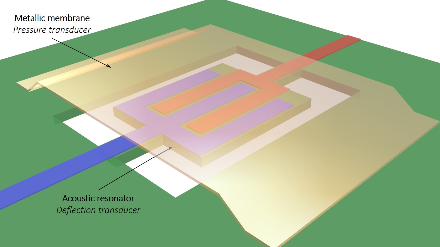
Piezoelectric micromachined ultrasound transducers (PMUTs) are suspended composite membranes capable of both sensing and sending sound waves that can interact with the environment of interest. They are used in a wide variety of everyday applications, from radar/sonar to non-destructive material testing and medical imaging. One emerging area of interest is in measuring acoustic spectroscopy. We want to do that in microfluidic channels by placing PMUTs above and below the channels. In this way, there is no influence on the sample as it flows along the channels and measurements are incredibly sensitive. In this project, the student will design and fabricate PMUTs with integrated microchannels.
|
 |
| Fig. 1 Schematic and working principle of PMUTs. Image taken from Qiu et al. | Fig. 2 SEM images of AlN PMUT from Lu et al. |
Project Components:
The main tasks involved in the project will be:
- Literature review of PMUTs and microfluidics (30% of the time – 3 weeks)
- Design and Fabrication of the resonators in CMi (50% of the time – 7-8 weeks)
- Microfluidic integration (20% of the time – 3 weeks)
Desired Skills:
- Fluency in English
- Autonomy
- Enjoys learning and facing new challenges
- Knowledge of cleanroom processes would be welcome
|
Type of Project: Section(s): Contact(s): |
Semester/Master Project Microengineering; Mechanical Engineering; Electrical Engineering |
 |
Semester/Master Project
|
The project
Suspended microchannel resonators (SMRs) consist of microfluidic channels embedded in vibrating structures (Fig. 1). Their configuration allows for a wide range of applications, from the rheology of homogeneous samples to the study of single biological analytes’ physical attributes.
So far, we have only fabricated SMRs in silicon nitride (SiNx, Fig.1 and 2), and we would like to shift our focus towards devices made of glass (SiO2). The main reason is the lower thermal conductivity of SiO2, which could help us achieve better sensitivity for calorimetry applications.
While the technology is mature for the fabrication of channels in silicon nitride, using glass as a structural material is more challenging. Indeed, the chemicals we use in our standard fabrication are not necessarily all compatible with glass, potentially requiring adjustments in the process flow.
|
 |
|
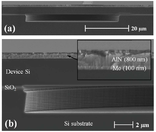
Fig. 1: SEM picture of an array of 2 SMRs made of silicon nitride at the end of the fabrication process (they are released). |
Fig.2 : SEM cross-sectional views of a silicon nitride channel after fabrication. The lateral walls are only about 260 nm thick. |
Project components
- Fabrication of the devices in CMi
- Characterization and inspection of the devices with the Scanning Electron Microscope (SEM)
- Design of lithography masks
- Fabrication of the piezoelectric electrodes and release
- Characterization and experiments
Desired skills
- Autonomy
- Cleanroom experience is welcome but by no means a necessity!
|
Type of Project: Section(s): Contact(s): |
Semester Project / Master Project Microengineering; Mechanical Engineering |
 |
Semester/Master project
|
The project
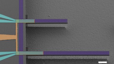
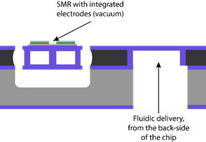
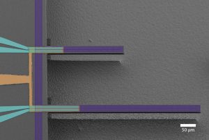
Microfluidic devices require appropriate packaging for the efficient delivery of fluidic samples. In particular, suspended microchannel resonators (SMRs, Fig. 1) need to be operated in a vacuum to boost their sensitivity. The combination of both vacuum encapsulation and fluidic delivery makes the packaging of such devices particularly challenging (see Fig. 2). Furthermore, our devices are driven and detected piezoelectrically, adding to the requirements and complexity of the packaging. At the moment, we are using a reversible in-lab modular interface for our experiments.
In this project, we would like to investigate a means to encapsulate those devices directly after the end of the fabrication. Before taking the devices out of the cleanroom, the devices should be sealed at wafer-level, before being diced into chips. We are looking for the most integrated possible solution.
|
|
|
Fig. 1: SEM picture of an array of 2 SMRs at the end of the fabrication process. The electrode tracks are depicted in orange and cyan and extend further away from the beams for wire-bonding. |
Fig.2: Schematic cross-section of the devices at the end of the fabrication. The vacuum is made around the devices on the top side, while the fluidic delivery is provided from the back-side. |
Project components
- Literature review of the existing wafer-level packaging methods
- Selection, fabrication, and characterization of a packaging method
- Experiments with the packaged SMRs
Desired skills
- Autonomy
- Cleanroom experience is welcome but by no means a necessity!
|
Type of Project: Section(s): Contact(s): |
Semester Project / Master Project Microengineering; Mechanical Engineering |
 |
Semester project
|
The project
The Center for MicroNanoTechnology (CMi) has installed a Nanoscribe Photonic Professional GT+ nano printer (https://www.epfl.ch/research/domains/cmi/cmi-home-page/equiment/photolithography/nanoscribe-photonic-professional-gt/). This tool works on the principle of two-photon absorption and can achieve features with resolution below 200nm.
We have already started to investigate the fabrication of microchannels with this nano-printer, with promising results (Fig. 1). The objective of this project is to optimize the fabrication of microchannels with thin walls and to develop a process flow in which we could create suspended structures. In addition, we would like to improve the fluidic network communicating with the channels, for fluidic delivery and experiments (Fig. 2).
|
 |
|
Fig. 1: SEM picture of 3D printed microchannels directly on silicon. Picture from Lénaïc Frehner’s semester project report. |
Fig.2: SEM picture of microchannels. Here, we attempted to print the fluidic network connecting the channels, but unsuccessfully. Picture from Lenaïc Frehner’s semester project report. |
Project components
- Design of microchannels with CAO software
- Fabrication and inspection of the microchannels in the cleanroom
- Development of a process flow allowing for the release of the devices
Desired skills
- Autonomy
- Cleanroom experience is welcome but by no means a necessity!
|
Type of Project: Section(s): Contact(s): |
Semester Project / Master Project Microengineering; Mechanical Engineering |
 |
Semester project
|
The project
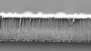
Since they are the first building block of all microfluidic devices, microchannels are of critical importance and interest and their design and fabrication require great care.
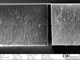
In recent developments, we have been exploring 2 different fabrication methods for the realization of those channels. The first method consists of using a sacrificial layer of poly-silicon that we etch to create trenches (Fig.1). After that, we deposit the structural material (usually silicon nitride) around the poly-silicon to encapsulate it, and we proceed to empty the channel. The second method is more straight forward, as we etch directly inside the silicon wafer before redepositing the structural material in the grooves (Fig. 2).
We are interested in learning more about the fabrication of the channels etched directly in silicon. We could focus on two aspects: the profile of the trenches when they are exposed to different chemistries and the effect of the crystallinity of the silicon wafer used.
|
|
|
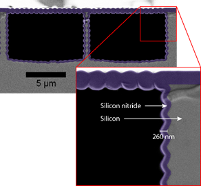
Fig. 1: SEM picture of a trench etched in poly-silicon (about 800nm wide). This is the first step in the fabrication of microchannels with the sacrificial material method. |
Fig.2: SEM cross-sectional views of a silicon nitride channel after fabrication. The channels were etched directly in the silicon. After the deposition of silicon nitride to close the channels, the lateral walls were only about 260 nm thick. |
Project components
- Design and fabrication of the microchannels
- Inspection of the channels with Scanning Electron Microscopy
Desired skills
- Autonomy
- Cleanroom experience is welcome but by no means a necessity!
|
Type of Project: Section(s): Contact(s): |
Semester Project / Master Project Microengineering; Mechanical Engineering |
 |
Master Project / Internship
|
The project
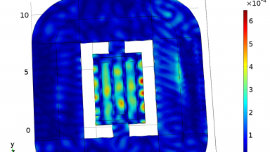
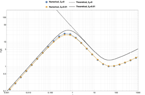
Suspended microchannel resonators (SMRs) consist of microfluidic channels embedded in vibrating structures. This configuration allows operation of the devices in a vacuum environment instead of immersed in the fluidic sample to analyze. Thanks to this, the damping losses are drastically reduced (increased quality factor) and the detection sensitivity is enhanced. Theoretical and experimental results have demonstrated that the energy dissipation is non-monotonic with respect to the viscosity of the fluid flowing in the resonator. In addition to that, a significant variation in the quality factor was discovered when the microfluidic channel axis was placed away from the beam neutral axis. The objectives of the project first consist in getting familiar with the literature, the results already obtained, and understand the Comsol model. Then, the project will be continued in order to complete the study (in particular, the behavior the devices with high-viscosity fluids needs to be investigated).
|
|
|
| Fig. 1: simulation of the first 2 modes of vibration of a Suspended Microchannel resonator. |
Fig. 2: non-monotonic behavior of the quality factor with respect to the viscosity of the fluid.
|
Project Components:
The main tasks involved in this project will be:
- Literature review
- Comsol modelling and simulations
Desired Skills:
- Autonomy
- Comsol knowledge would be welcome
|
Type of Project: Section(s): Contact(s): |
Master Project / Internship Microengineering; Mechanical Engineering |
Acoustic mode resonators
![SEM image of a µTag internalized by the cell. [Ref] H. Wong et al, PhysRev Applied, 2017](https://nems.epfl.ch/wp-content/uploads/2018/10/FM_CellProject2_pic1.png) |
Master Project You will do mostly Design and Fabrication We want to probe cell properties from the inside |
Master project
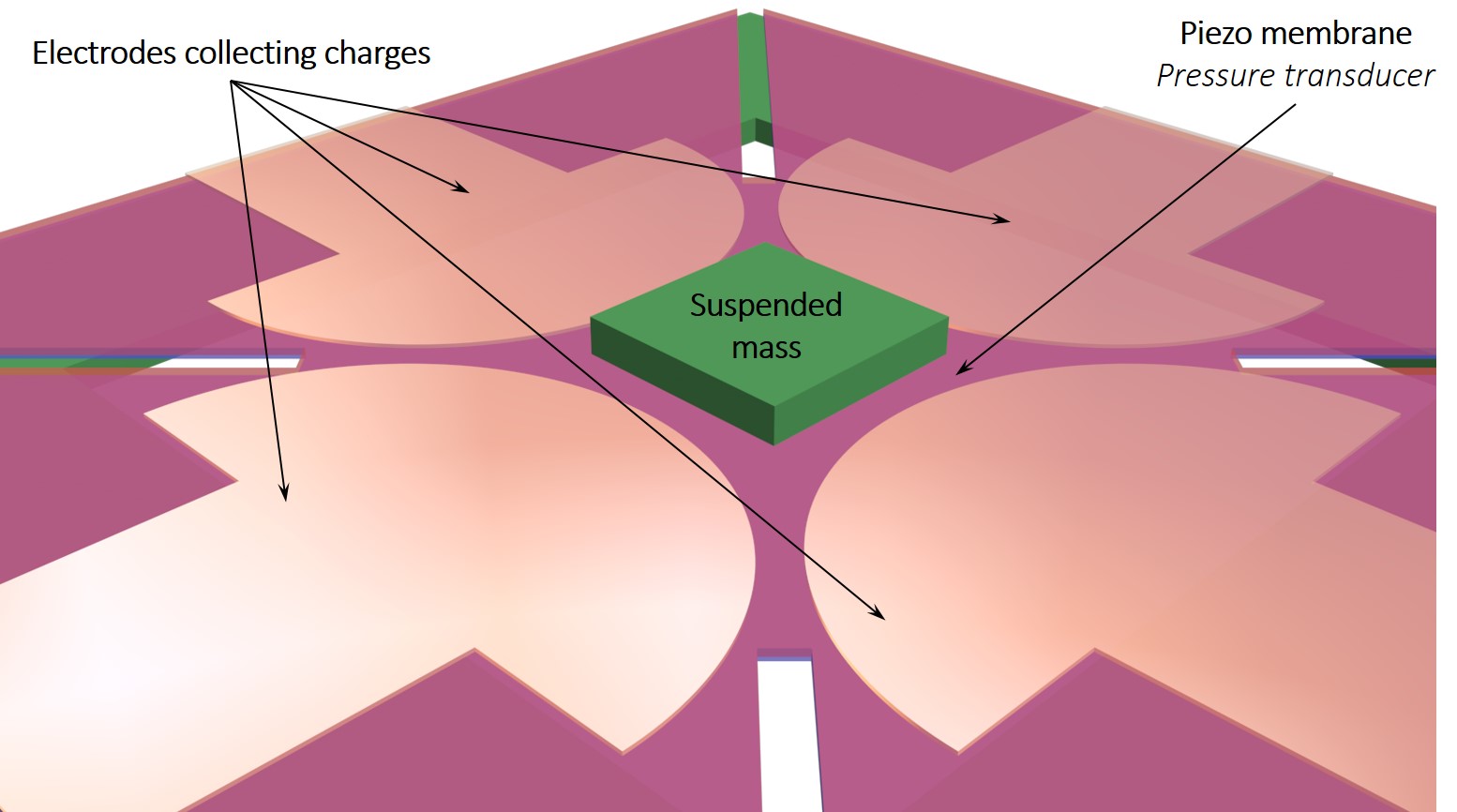
Recently, a number of cell probing techniques have been developed to study the behaviour and properties of a single cell. Most of them are invasive or require optical detection. The goal of the project is to develop a wireless cell-probing system similar to an RFID system that will identify and track the movement of an individual cell in real time. Fig. 1 shows the insertion of such small device in a mouse macrophage (white blood cell). The idea is to use a piezoelectrically actuated acoustic resonator as an RFID tag that should be small enough to easily internalized and be efficient enough to send back the data from inside the cell. However, little work has been conducted to realize the full potential of acoustic devices with critical dimensions less than a few microns. The main goal of the student will be to fabricate LAMB wave resonators on thin film lithium niobate (Fig. 2). The student will get hands on experience with different microfabrication tools related to e-beam lithography, wet/dry etching and metrology.
|
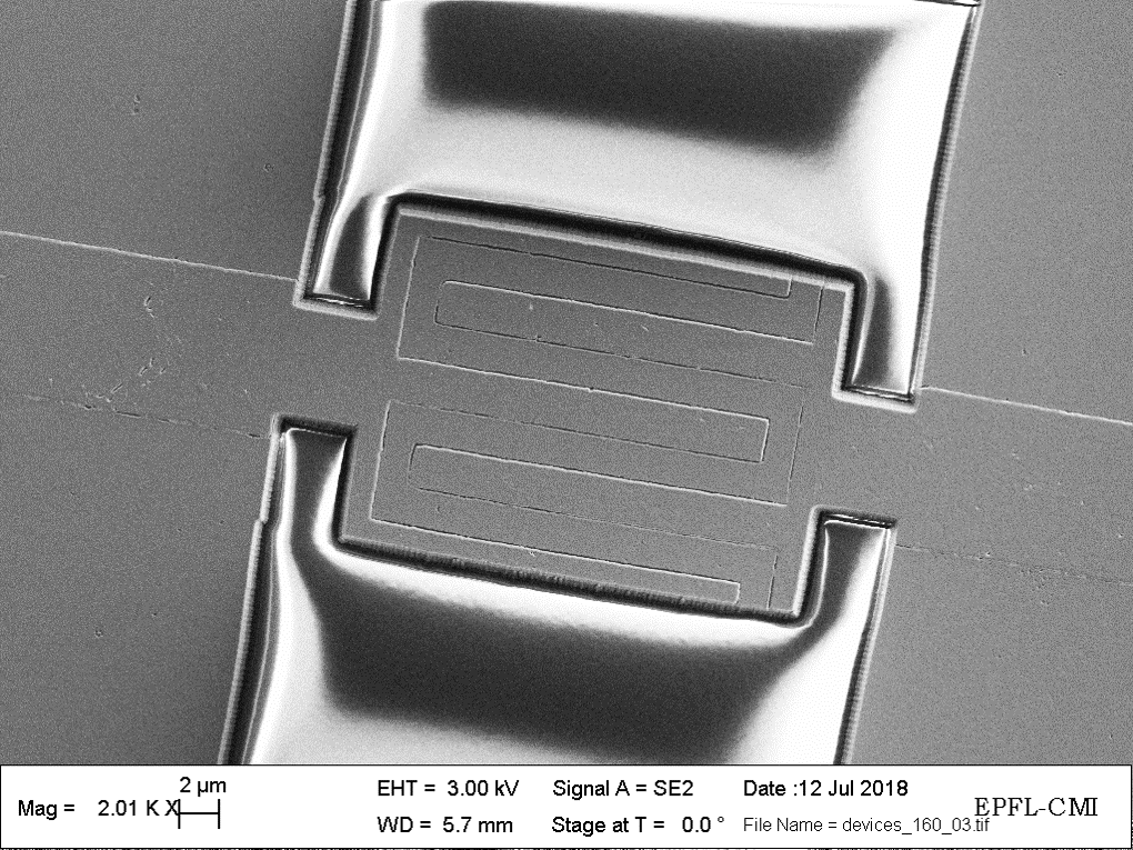 |
| Fig 1: SEM image of a µTag internalized by the cell [Ref] H. Wong et al, PhysRev Applied, 2017. | Fig. 2: SEM image of a fabricated miniaturized acoustic resonator. |
Project Components:
The main tasks involved in the project will be:
- Literature review of LAMB wave resonators including S0 and SH0 modes (10% of the time – 1-2 weeks)
- Related cleanroom trainings at CMi (10% of the time – 1-2 weeks)
- Design and fabrication (60% of the time – 8-9 weeks)
- Characterization of fabricated devices (20% of the time – 2-3 weeks)
Desired Skills:
- Fluency in English
- Autonomy
- Interested in microfabrication
- Knowledge of MEMS is desirable
|
Type of Project: Section(s): Contact(s): |
Master Project Microengineering; Mechanical Engineering; Electrical Engineering |
 |
Master Project You will mostly do Simulation and Fabrication We want to analyze bio samples via acoustic waves |
The project
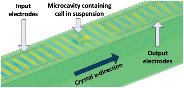
Acoustic spectroscopy is being increasingly used to characterized different bio-materials and for the detection of biomolecules. The idea is to design and fabricate a miniaturized platform for the detection and characterization of cancerous cells by using Surface Acoustic Waves (SAW). The proposed platform consists of a pair of Interdigital electrodes (IDTs) for the generation and reception of SAW waves with an embedded microchannel in between for the trapping of cells or other biological entitiesas shown in Fig. 1. Information such as the elasticity of the sample, can be determined by measuring the phase change of the resultant SAW waves after passing through the sample.
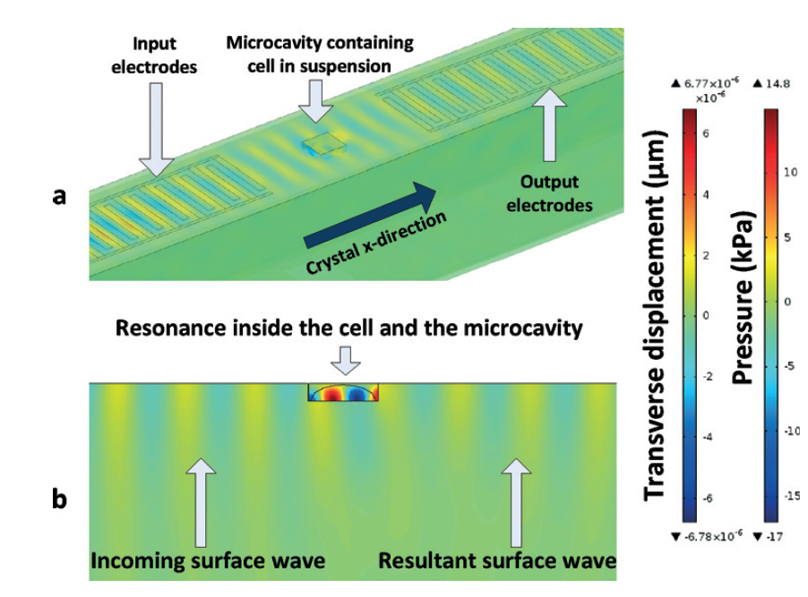 |
Fig 1: (a) 3D simulation model. (b) Cross-sectional image from the central axis of a microcavity. Ref.: R. J. Cote and O. Tigli, Lab on a Chip interrogation of single tumour cells in Lab Chip, vol. 16, pp. 163-171, 2016. |
Project Components:
The main tasks involved in the project will be:
- Literature review of SAW-based acoustic spectroscopy (25% of the time – 3-4 weeks)
- Design and FEM modelling of the proposed platform (25% of the time – 3-4 weeks)
- Fabrication of the resonators in CMi (40% of the time – 5-6 weeks)
- Preliminary characterization of the resonators (10% of the time – 1-2 weeks)
Desired Skills:
- Fluency in English
- Autonomy
- Enjoys learning and facing new challenges
- Knowledge in cleanroom processes is a plus
|
Type of Project: Section(s): Contact(s): |
Master Project Microengineering; Mechanical Engineering; Electrical Engineering |
In previous simulations performed in ANEMS, we have studied the behavior of PAW resonators in vacuum, however we would like to explore the possibility of using these devices for different biological applications where liquid environments are inevitable. With this project we aim to study how the viscous damping affects the QF, and assess the viscous losses in different biological mediums such as: cell medium, blood, phosphate buffer solution etc. Furthermore, we want to learn how the design can be improved and optimized to minimize the dissipative effect caused by the surrounding fluid.
Simulations will be performed on COMSOL: you will set up the coupling between the solid-liquid interface and carry out parametric sweeps to optimize the design.
 |
Project components
- Familiarize with COMSOL and the existing FEM model of PAW resonator
- Familiarize with coupling solid-liquid interface in COMSOL
- Literature review on properties of the different biological mediums
- Optimization of device performance for different biological environments
Desired skills
- Experience using COMSOL is welcome but by no means a necessity!
|
Type of Project: Section(s): Contact(s): |
Semester/Master Project Microengineering, Mechanical Engineering, Bioengineering, Electrical Engineering |
The project
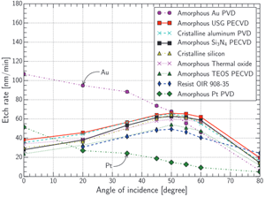
Ion Beam Etching (IBE) is a process that removes material from an exposed surface through bombardment of inert ions. Other etching processes such as chemical or reactive ion etching rely on chemical reactions with the etched material. For that reason, these processes are typically limited to a few materials that can react with the etchant species. On the other hand, IBE can be used to etch any material, even inert ones, due to the purely physical nature of the process. The etch rate of IBE etching depends on i) the material to be etched and ii) ion energy and incidence angle.
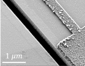
In our group, we use IBE to etch AlScN, LiNbO3 and various metals to fabricate piezoelectric resonators (Fig. 1). To get an optimal profile of the etched features, we need to know the angular dependence of the IBE etch rate.
The project’s objective is to characterize the angular dependence of the IBE etch rate for several materials including AlScN, LiNbO3 and SiO2 (Fig. 2). The secondary objective is to develop a numerical model to simulate the evolution of the profile of the etched feature.
References:
[1] S. Stettler and L. G. Villanueva, “Optimization of Edge Profile for Improved Anti-Resonance Quality Factor in Lithium Niobate SH0 Resonators,” 2022 IEEE International Ultrasonics Symposium (IUS), 2022, pp. 1-4, doi: 10.1109/IUS54386.2022.9957511
[2] N. Gosset et al, “Single and multilayered materials processing by argon ion beam etching: study of ion angle incidence and defect formation”, 2015 J. Micromech. Microeng. 25 095011
 |
 |
|
Fig. 1: Trench machined with IBE into LiNbO3 to define the outline of an acoustic resonator [1] |
Fig. 2: Etch rates of different materials as a function of the angle of incidence between the argon ion beam and the substrate holder [2] |
Project components
- Literature review (1-2 weeks)
- Processing of material samples in the ion beam etcher and characterization of the etch rate with various metrology tools in the cleanroom (6-7 weeks)
- Developing numerical model and experimental validation (4-5 weeks)
Desired skills
- Ability to work independently
- Processing in the cleanroom demands a meticulous and organized way of working.
- Fluent and comfortable speaking English
- Basic coding skills in MATLAB or Python for the modelling part.
|
Type of Project: Section(s): Contact(s): |
Semester/Master Project Micro engineering, Electrical engineering, Mechanical engineering, Material science, Chemical engineering |
Thin Film Optimization
 |
Semester/Master Project You will do Theoretical study and Fabrication We want to obtain the best PZT layers |
The project
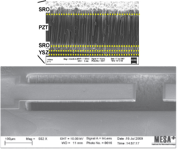
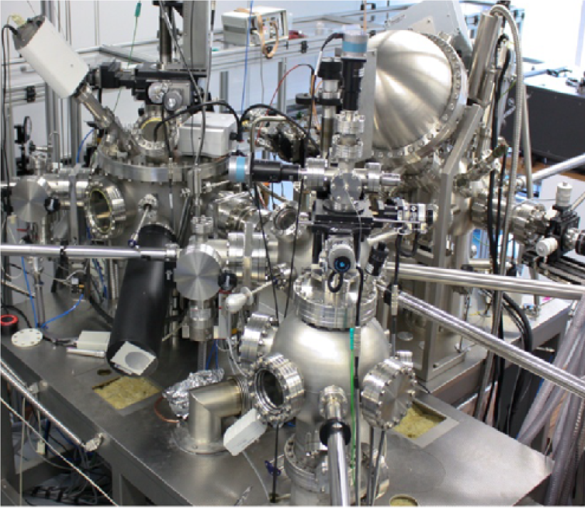
Piezoelectric materials, such as lead zirconate titanate (PZT) and aluminum nitride (AlN), are the mainstay materials in MEMS for efficient actuation and sensing applications. When moving from the established MEMS fabrication to NEMS, consistent deposition of highly piezoelectric, nanometer-thick films becomes increasingly important. Several different deposition methods are possible for PZT, including sol-gel processing, sputter deposition and pulsed laser deposition (PLD). Of the three, PLD offers the opportunity to deposit epitaxial, stoichiometric PZT at high temperature. PLD is a physical vapor deposition, using a pulsed laser to vaporize the material of interest off a target onto a substrate in an ultra-high vacuum chamber. Depositing high-quality PZT thin films requires heavy optimization of the deposition parameters, high purity targets and proper substrates for epitaxial growth. In this project, the student will study PLD, piezoelectricity and PZT and contribute to the deposition and fabrication of PZT in CMi.
 |
|
| Fig 1 Example of PLD system capable of depositing PZT Reference: D. H. A. Blank, M. Dekkers, and G. Rijnders, “Pulsed laser deposition in Twente: from research tool towards industrial deposition,” J. Phys. D. Appl. Phys., vol. 47, no. 3, p. 34006, 2014. | Fig. 2 Above, cross-sectional SEM image of PLD-grown PZT on an SRO/YSZ electrode. Below, SEM image of released PZT-based cantilever. Reference: M. D. Nguyen et al., “Characterization of epitaxial Pb(Zr,Ti)O 3 thin films deposited by pulsed laser deposition on silicon cantilevers,” J. Micromechanics Microengineering, vol. 20, no. 8, p. 85022, 2010. |
Semester Project Components:
The main tasks involved in the project will be:
- Theoretical study of piezoelectricity, PZT, PLD
- Introduction to CMi and installed PLD machine
- Optimizing PZT deposition and dry etching in cleanroom
Desired Skills:
- Fluency in English
- Autonomy
- Enjoys learning and facing new challenges
- Knowledge in cleanroom processes is a plus
|
Type of Project: Section(s): Contact(s): |
Semester/Master Project Microengineering |
Reactive-Ion Etching
Topic
One of the main steps of every microfabrication process is the removal of the unwanted parts of a film to transfer the pattern of the mask on the substrate. Etching procedures can be divided in two main groups: wet etching and dry etching. Wet etching uses an aggressive chemical liquid solution to remove the substrate parts, while dry etching employs either a gas or a plasma. Plasma etching allows for a mixed chemical and physical action, called Reactive Ion Etching. The chemical action is strengthened by a physical bombardment of ions on the substrate to improve the verticality of the etching process.
Project
Between all the semiconductor materials used in MEMS Aluminum Nitride is interesting because of its piezoelectric effect and compatibility with standard IC production processes. AlN filters are widespread in RF frontends since the end of 20th century. To comply with the requirements of bandwidth in 5G it is necessary to increase the piezoelectric coefficient of AlN, which is achievable with alloying with Sc. One of the downsides in shifting from AlN to AlScN it is that Sc is much more resistant to etching, requiring to optimize the process shifting towards more aggressive chemistries and higher power.
The most widespread plasma etching of AlN is done with an inductively coupled plasma (ICP) with Chlorine chemistry. EPFL Centre of microtechnology (CMi) employs such a standard process, but more modern machines are to be tested.
The PTSA ICP SI 500 etcher from Sentech allows for control of chemistry, power, and temperature of the chamber, allowing for exotic recipes to be developed. Aim of the project is to investigate the etch rate, selectivity, and sidewall verticality of the etched AlN and AlScN.
Project components
The main tasks involved in the process will be:
- 10% of time review of ICP
- 10% in training for machines
- 30% in process develpment
- 50% of time in measurements
Required skills
- Fluency in English or French
- Interest in microfabrication
Desirable skills
- Knowledge of basic microfabrication processing
Type of project: Master/Semester
|
Type of Project: Section(s): Contact(s): |
Semester/Master Project Microengineering, Electrical Engineering, Physics |
The project
Ferroelectric materials belong to a subset of piezoelectric materials where an observable spontaneous polarization can be reversed by applying an electric field, similarly to ferromagnetic materials when a strong enough magnetic field is applied.
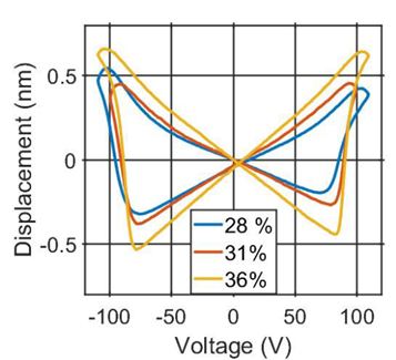
Aluminium-Scandium Nitride, a promising material for piezoelectric MEMS resonators fabrication, shows ferroelectric behaviour at high Sc to Al concentrations (above 27% Sc/Al atom ratio[1]) which opens a new field of study on the effect of ferroelectric domains on the piezoelectric properties and allows to fabricate self-switching filters for RF telecommunications.
The project investigates the ferroelectric properties and the effects of High voltage poling on a thin film. Ferroelectric polarization will be used as a characterization technique, to investigate the coercive field of high Sc concentration AlScN and the displacement curves, and as a switching technique for resonators, to investigate the change of electrical and crystalline properties after poling
|
|
|
|
Fig. 1: Butterfly curve of displacement of a ferroelectric thin film, as a function of voltage for different Sc concentrations [2] |
Fig.2: PUND (Positive-Up-Negative-Down) response of a ferroelectric thin film [2] |

References:
[1] S. Fichtner, F. Lofink, B. Wagner, and T.-N. Kreutzer, “Ferroelectricity in AlScN,” p. 2.
[2] M. Pirro, B. Herrera, M. Assylbekova, G. Giribaldi, L. Colombo, e M. Rinaldi, «Characterization of Dielectric and Piezoelectric Properties of Ferroelectric AlScN Thin Films», in 2021 IEEE 34th International Conference on Micro Electro Mechanical Systems (MEMS), gen. 2021, pagg. 646–649.
Project components
- Thin film analyzer setup and introduction to high voltage measurements and safety
- Measurement of polarisation curves and displacement (LDV integration)
- Poling and de-poling switching and electrical measurements
Desired skills
- If some particular skills are desirable list them here
|
Type of Project: Section(s): Contact(s): |
Semester/Master Project Mechanical engineering (IGM), Material Science (IMX), Electrical and Micro Engineering (IEM) |
Semester (or Master) project
The project
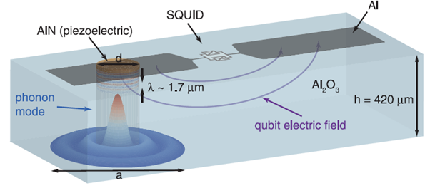
Quantum computing promises to be the next revolution in the field of information processing and telecommunications. The information carrier of quantum computing is called a qubit, and recent advancement in the technology to improve the generation of qubits with circuit quantum electrodynamics (cQED) has brought to attention the advantage of hybrid systems where qubits can be coupled to acoustic resonators to improve their coherence time[1] and make quantum states with substantial masses[2].
Piezoelectric materials allow for strong coupling between the electric field of the superconducting qubit and the acoustic wave sustained in a mechanical resonator, to increase the coherence time of the qubit. Given the operating conditions (mostly cryogenic temperatures required for the superconducting qubit to be generated), the deposition process for the piezoelectric thin film must be adapted for those materials mostly used in the field.
The process will be centred on the exploration of the sputtering processes to deposit superconductive electrodes and piezoelectric thin films adapted for quantum acoustics.
References:
[1] Y. Chu et al., “Quantum acoustics with superconducting qubits,” Science, vol. 358, no. 6360, pp. 199–202, Oct. 2017, doi: 10.1126/science.aao1511.
[2] M. Bild et al., “Schrödinger cat states of a 16-microgram mechanical oscillator,” Science, vol. 380, no. 6642, pp. 274–278, Apr. 2023, doi: 10.1126/science.adf7553.
|
|
|
Fig. 1: Example of a hybrid Qubit system from [1] |
Project components
- Investigation of superconductive materials and deposition techniques
- Deposition of superconductive material and conductivity test
- Deposition of piezoelectric material and characterization
Desired skills
- Knowledge about PVD techniques, especially sputtering and reactive sputtering
|
Type of Project: Section(s): Contact(s): |
Semester/Master Project Section of Microengineering, Section of Electrical Engineering, Section of Quantum Science and Engineering |
Complex Dynamics
 |
Semester/Master Project You will mostly do Circuit Design We want to find the best platform to characterize NEMS |
The project
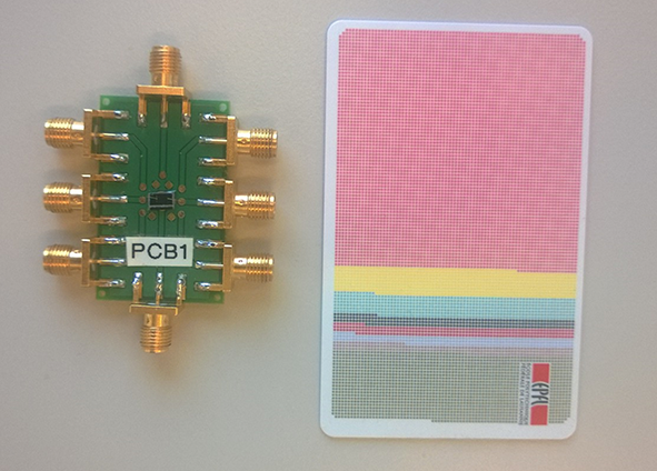
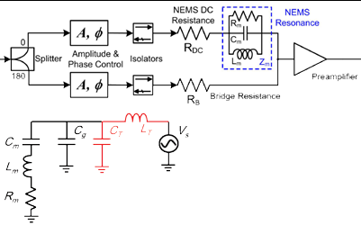
NEMS have a large potential for sensing applications due to their size. However, at the same time, NEMS are difficult to integrate with electronics due to huge impedance mismatching and poor amplification. In this project, a circuit will be designed with background cancellation capabilities and/or impedance matching. Then, in collaboration with the Electronics Workshop, a PCB will be modelled, designed and fabricated that can be used to make measurements of a NEMS device. For the modelling, an equivalent circuit will be created to analyze the impedance matching network and amplification stage for the best integration with NEMS.
 |
|
| Fig. 1 Equivalent Circuits with NEMS Resonator and (top) a balancing bridge and (bottom) a LC-tank. | Fig. 2 PCB with NEMS device in center. Camipro card for scale. |
Project Components:
The main tasks involved in the project will be:
- Literature review of existing methods (20% of the time – 3 weeks)
- Design of circuit, including resonator model (40% of the time – 6 weeks)
- Fabrication of the PCB (20% of the time – 3 weeks)
- NEMS characterization (20% of the time – 3 weeks)
Desired Skills:
- Fluency in English
- Autonomy
- Enjoy learning and facing new challenges
- Knowledge of analog circuit design is a plus (even a must)
|
Type of Project: Section(s): Contact(s): |
Semester/Master Project Electrical Engineering, Microengineering; Mechanical Engineering |
 |
Semester/Master Project You will do Simulations, Fabrication and Characterization We want to understand the most complex devices. |
The project
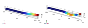
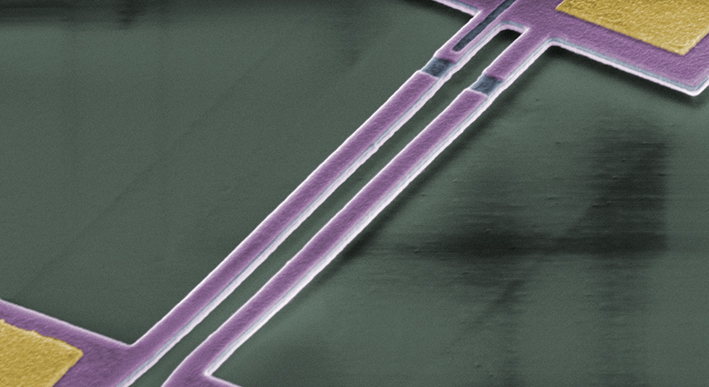
Coupling phenomena can be found in most of physical systems in nature. Coupling increases the systems’ dimensionality (making the systems more complex) and, in some cases, also the functionality (making the “whole greater than the sum of its parts”). In Nano-electromechanical Systems (NEMS), coupling between neighboring devices can be achieved, for example, via mechanics. A common ledge (support) for different devices will effectively couple them, and therefore collective dynamics might emerge. It is necessary, however, that this coupling is strong enough so that the devices actually “coupled”. It is the purpose of this project to analyze how the strength of this linear coupling depends on the physical constraints that act on adjacent devices. This will be studied using directly as well as parametrically driven responses.
| Fig. 1: Coupled piezoelectric NEMS using the overhanging ledge in one of the anchoring points. Individual dimensions are 9µm*450nm*210nm. | |
Project Components:
The main tasks involved in the project will be:
- Simulation and analytical calculation of coupling coefficients (30% of the time – 4-5 weeks)
- Design and fabrication of a battery of devices (50% of the time – 7-8 weeks)
- Characterization of the frequencies, quality factors and coupling rates (20% of the time – 3 weeks)
Desired Skills:
- Fluency in English
- Autonomy
- Enjoy learning and facing new challenges
- Knowledge of Finite Element Modelling is a plus
|
Type of Project: Section(s): Contact(s): |
Semester/Master Project Microengineering; Mechanical Engineering; Electrical Engineering |
The project
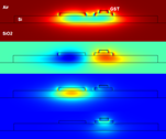
Reconfigurable Silicon Integrated Photonic Circuits (PICs) enable the construction of increasingly complex optical networks on a chip. Of particular interest are non-volatile photonic components [1]: a finite actuation pulse toggles their state, with no further action required to maintain the desired state. Integrating chalcogenide phase change materials (PCM) on silicon photonic can provide this functionality, since these alloys have extremely different optical properties in crystalline or amorphous solid states, with state transitions possible with nanosecond-duration heat pulses.
Our recent research has aimed at designing PCM optical integrated components and developing a process flow for their fabrication at the CMi using the DUV Stepper as the only lithography method. This will allow demonstrating scalable PCM-PICs, apt for reliable and straightforward production with integrated electrical actuation.
A crucial step for the manufacture of PCM PICs is the careful design of the exposure reticle, the mask used by the DUV Stepper. In this project you will contribute to the construction of a complex multi-layer DUV Stepper reticle layout for the realization of a wide range of prototype optical components and their parametric variations. Optical and thermals aspects of some components may still need to be evaluated using 2D/3D COMSOL models.
 |
|
Fig. 1: Simulated modes for coupled silicon waveguides with PCM in amorphous and crystalline state. |
Project components
- Study of a fabrication process flow for integrated photonics with PCM on the DUV Stepper (10% 1-2 weeks).
- Realization of a DUV stepper reticle layout for a PICs prototype, using dedicated software. (60%, 8-9 weeks)
- Automatic generation of individual components and chip layout assembly.
- Writing of a reticle at CMi (photolithography).
- Modelling and analysis of photonic components with PCM materials. (30%, 3-4weeks)
- Thermal transient simulation
- Optical simulation
Desired skills
- Basic programming skills (Matlab is a plus).
- Knowledge in optics/photonics is a plus.
- Experience with COMSOL modelling is a plus.
- Motivated, autonomous, problem-solver.
|
Type of Project: Section(s): Contact(s): |
Semester/Master Project MT, MNIS, others possible |