Micro- and nano-fabrication is key to research in nanophotonics, where the structures of interest have dimensions ranging from a few nanometers to several microns. Over the years, we have developed many different technologies, with emphasis on metallic nanostructures.
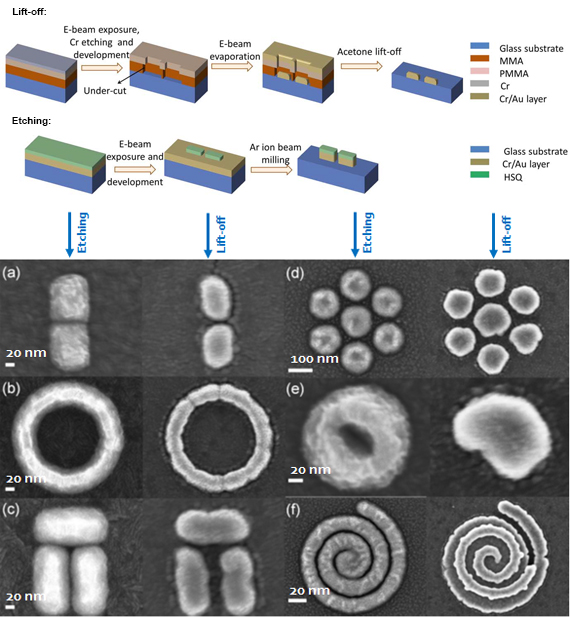
Etching vs. lift-off
Nanostructures are fabricated using electron beam lithography to define the structure shape into a resist, as illustrated below. Most nanostructures are fabricated with a lift-off technique, where a positive tone resist is used and cavities appear in the resist after exposure and development. Then, the nanostructures’ metal is deposited inside those cavities and the surrounding material is dissolve into acetone. Recently, we have developed another approach based on negative tone resist, that remains after development wherever it has been exposed. This resist is then used as hard mask to etch the surrounding material. The bottom part of the figure compares both techniques on a variety of Au nanostructures and demonstrates the superior quality of nanostructures obtained by etching, where features as small as 10 nm can be realized!
Hybrid nanostructures and metasurfaces
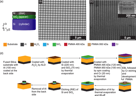
An interesting feature of etching is that relatively thick nanostructures can be realized, this is not the case with lift-off since the cavity formed in the resist becomes clogged during metal evaporation. Furthermore, it is possible to fabricate hybrid nanostructures that include different materials, since they are deposited at the beginning of the process and can be etched successively at the final step. The following figure illustrates a metasurface that was fabricated this way, with meta-atoms consisting of a Si cylinder and an Al disk separated by a SiO2 spacer. The process is quite intricate and the Al disk serves both as etch mask during the process and as plasmonic element for the metasurface.
Keeping your silver shiny!
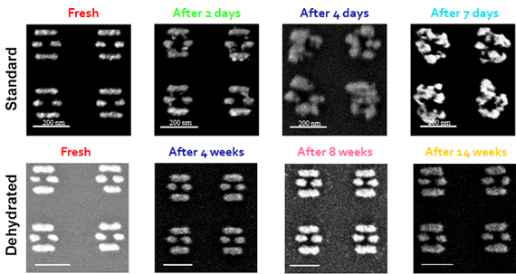
Most plasmonic nanostructures are fabricated in Au because it is relatively easy to work with and is very stable. Unfortunately, absorption is very high in Au, which limits the field enhancement and produces spectrally broad resonances. To overcome this, we have developed recipes for the fabrication of nanostructures in Al and Ag. Both metals are extremely interesting for plasmonics, both in the linear and nonlinear regimes. Unfortunately, Ag has a major drawback: it rapidly deteriorates. If you have silver cutlery, you certainly know that it needs to be polished, otherwise it turns dark. It is believed that sulfur in the ambient air could be responsible for this; however, we have demonstrated that actually humidity is playing the key role in Ag deterioration. With this observation, came also the cure: a dehydration technique that can keep Ag nanostructures perfect over months, as illustrated in the figure below.
Low temperature annealing
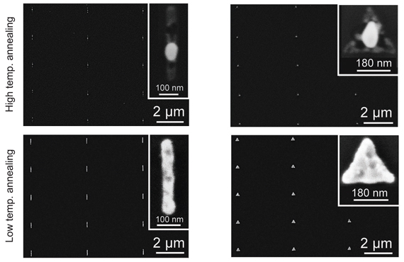
The choice of plasmonic metals is quite limited: Au, Ag, Al, W, Cu, which restricts the possible spectral range where these effects can be used. To overcome this limit, we have recently investigated the utilization of Au-Ag alloys with different stoichiometry. As we change the proportion of Au and Ag, we change the dielectric function and can explore novel plasmonic materials in the range between Au and Ag. Unfortunately, alloying is performed at high temperature (800-900 °C), which destroys the shape of the nanostructures that become simple round drops, as illustrated below on the top row. We have demonstrated a low temperature alloying technique at only 300°C for 8h followed by 30 min at 450°C, which produces a perfect alloying and does not destroy the nanostructures, as illustrated on the bottom row.
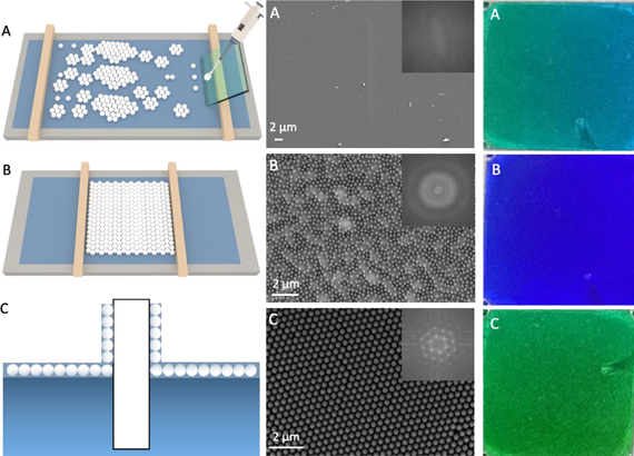
Colloidal lithography
Electron beam lithography enables the realization of nanostructures with arbitrary shapes. Unfortunately, it is difficult to produce a very large number of such structures since the writing process is sequential, one structure after the other. To address this issue, we also develop techniques that can fabricate nanostructures on a very large area, colloidal lithography that can be used to cover a full wafer with nanostructures in a single step. The principle is illustrated below on the left column: polystyrene spheres are floated on the surface of water in a Langmuir-Blodgett trough. The wafer is immersed in the liquid and as it is retracted the polystyrene spheres organize into a closely packed arrangement on its surface. The middle column shows some typical spheres’ arrangements. These spheres can be used as template for the subsequent fabrication of nanostructures on the entire wafer, producing some interesting color effects, as illustrated in the right column.
Most nanofabrication takes place at the EPFL Center of MicroNanoTechnology (CMI), which provides an outstanding infrastructure in over 500 square meters of class 100 and 1000 clean rooms. The center is equipped with modern and powerful processing machines and managed by a very competent staff.