Silicon-based heterojunctions and transparent contact materials
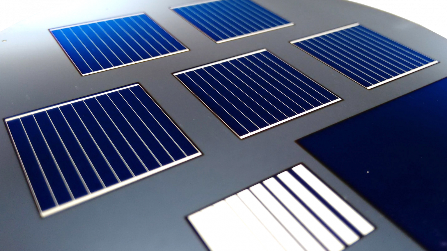
Silicon heterojunction solar cells typically require three layers of thin film material on each side of a silicon wafer to create the charge-carrier-selective contacts that allow conversion of sunlight into usable electricity. This conversion starts with photon absorption that generates an electron/hole pair, and is followed by selective collection of each of these charge carrier at spatially separated locations. Multiple losses can occur along this process, and the continuous solar cell efficiency improvement experienced in the last three decades required identification and addressing of each of these losses. Some losses are still to be addressed to harvest fully the potential of these devices, many of them due to fine interface properties. We perform extensive solar cell characterization to unravel the limitations of state-of-the-art devices and further extend the learning curve of silicon heterojunction technology [Tomasi2017, Haschke2018].
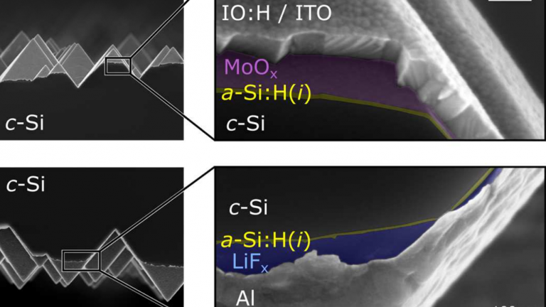
Triggered by other photovoltaic technologies such as organics, a whole field of research aiming at replacing the traditional thin-film-silicon-based contact layers in silicon heterojunction solar cells with better counterparts emerged. The aim is to achieve higher solar-cell efficiencies with simpler processing. Our take on this topic is to integrate materials already shown to form selective contacts on state-of-the-art devices, and then clarify their limitations. With dedicated processes and characterization, the potential of these materials can be assessed. Currently investigated materials typically include MoOx and ZnO [Bullock2018, Wu2018].
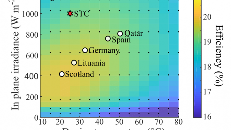
Solar cells and modules are generally characterised at—and thus optimised for—standard test conditions (STC), which correspond to a temperature of 25 °C and an illumination of 1000 W/m2 with the AM1.5G spectrum. However, these conditions very rarely correspond to the actual operating conditions in the field: depending on the location, solar cells experience higher temperatures and/or lower illumination than STC. Such changes of operating conditions have implications on the solar cell performances, and the device architecture outputting the most energy per square meter over a year is not necessarily the optimal one when measured in the lab. With a characterization setup and yearly energy calculation routine both developed in-house, we study the climate-specific performance of solar cells and provide guidelines for maximal energy production [Haschke2016, Cattin2019 (in preparation)].
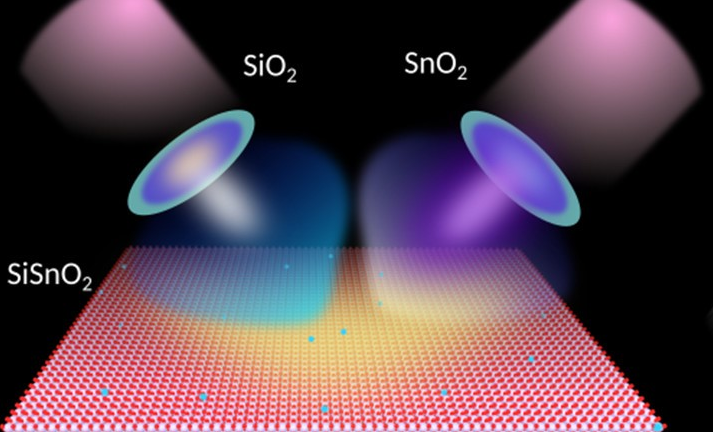
We strive to demonstrate the experimental fabrication of promising optoelectronic materials. We particularly focus on transparent electrodes with application-targeted transparency/conductivity properties such as Zr-doped indium oxide or indium-free mixed cation oxides such as ZTO. We also investigate low-temperature plasma-assisted synthesis of computationally promising p-type transparent conducting materials as well as III-V semiconductors such as BP, GaN and GaP [Morales-Masis2017, Rucavado2018].
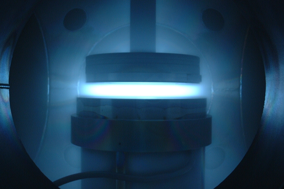
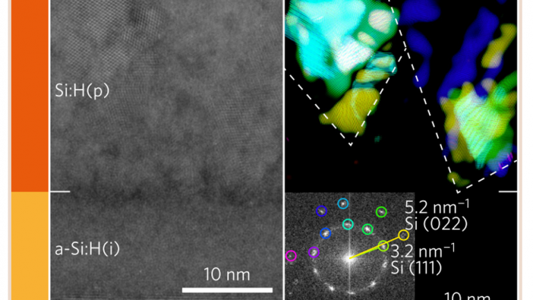
With a suite of 15 plasma-enhanced chemical vapor deposition reactors and three reactive sputtering chambers, we extensively use plasmas to synthesize functional layers at low temperature. Materials investigated include silicon and silicon alloys, III-V semiconductors and metal-oxides (both as transparent electrodes and as contact layers). We use optical emission spectroscopy and infrared spectroscopy to analyze the plasma, and determine the conditions leading to specific film properties, from insulating to highly conducting and from amorphous to nanocrystalline [Bugnon2012, Bartlome2015].
Please note that the publication lists from Infoscience integrated into the EPFL website, lab or people pages are frozen following the launch of the new version of platform. The owners of these pages are invited to recreate their publication list from Infoscience. For any assistance, please consult the Infoscience help or contact support.