Facilities
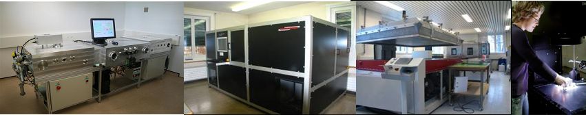
The laboratory bases its research on an impressive technology park including 9 PE-CVD systems, 6 systems for the deposition of TCO’s and metallic layers and 2 systems for plasma etching. Samples with sizes ranging from a few mm up to 40×50 cm² can be processed. The laboratory versatile laser scribing system for monolithic integration of PV modules. For cristalline silicon technology the lab is equiped with wet etching bench, screen printing equipment and annealing furnace. As part of IMT, the lab has access to the clean room facilities of the Comlab.
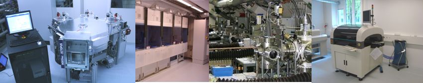
Extensive measurement systems allow for the characterization of semiconductor and optoelectronic layers, as well as for the performance testing of devices ranging from thin-film sensors to single-junction and tandem solar cells. Optical measurements and defects spectroscopy include reflection, transmission, ellipsometry, angular resolved, scattering, PDS, and FTPS. The lab is operating large area dc (22×22 cm²), dual lamp, Wacom simulator, spectral response, infrared lock-in thermography and variation thereof, and photo-luminescence and electro-luminescence.
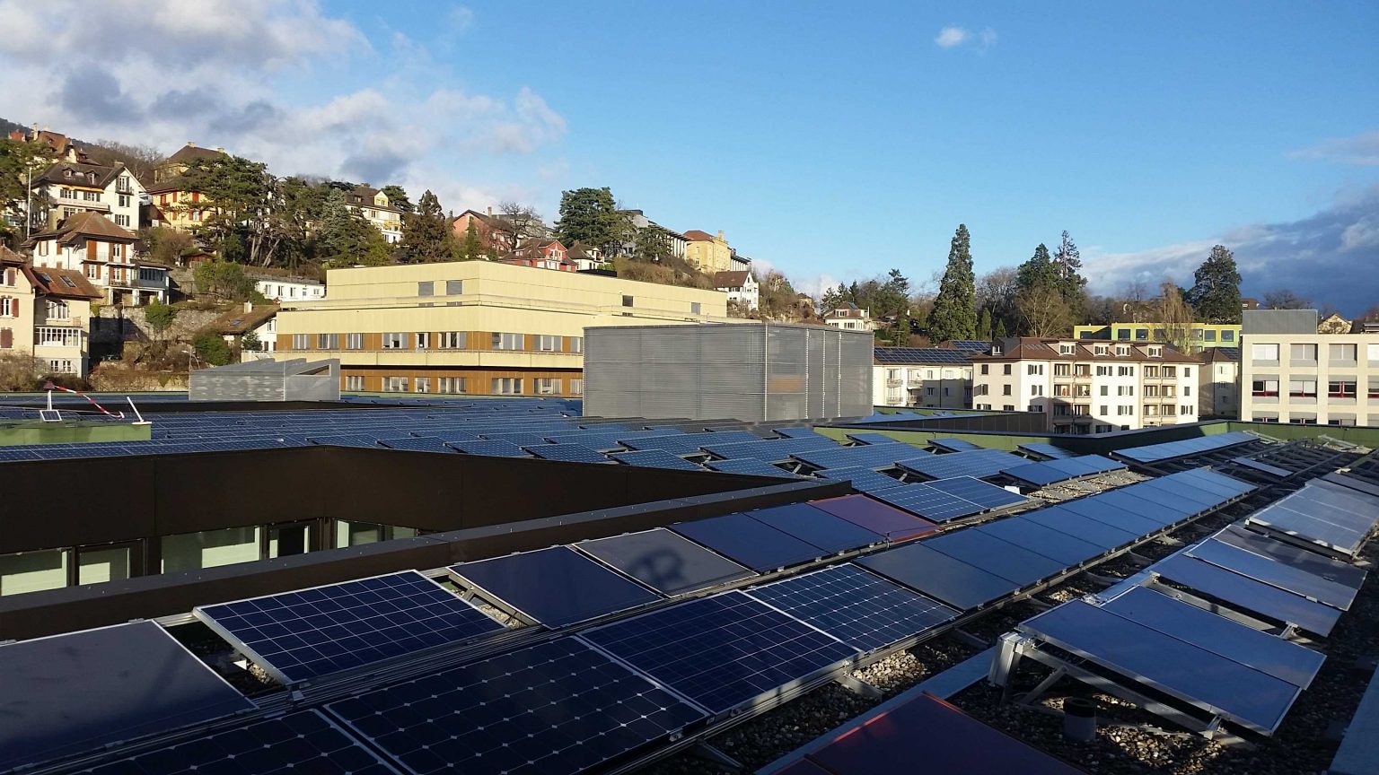
The lab is fully equipped for large area module technology processing, reliability testing, and module measurement.
Recent aquisitions:
A new versatile CVD deposition tool for coating applications has been aquired in 2013. This tool will allow for larger process parameter range (25°C-600°C; 0.5-250 mbar, low flow and high flow) and a variety of material thanks to its coupling with a remote plasma source and a UV illumination source.
An Oerlikon Clusterline 200 system for physical vapor deposition (PVD) has been acquired at the PVLab and is fully operational since March 2013. The tool is equipped with 2 loadlocks, an automatized transfer system and 4 individual processing modules. The individual modules allows the development of different materials: from transparent conductive oxides (TCOs) , metals and dielectric coatings.