Overview
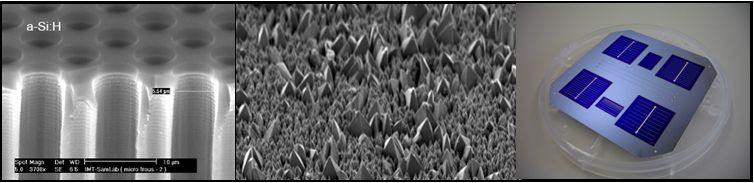
The Photovoltaics-Laboratory (PV-Lab) of IMT, founded in 1984 by Prof. Arvind Shah and headed by Prof. Christophe Ballif since 2004, has pioneered several new processes for the preparation of thin-film silicon, such as the introduction of very high frequency (VHF) plasma deposition and microcrystalline silicon as an efficient photovoltaic material, and simple processing of heterojunction crystalline cells. Current activities of the laboratory cover a broad spectrum, ranging from fundamental research to industrial technology transfer. The laboratory employs currently over 40 people. Example of highlights include the realisation of tandem solar cell – perovskite on p-type c-Si – with an efficiency over 25%. In 2012 The PV-lab supported the creation of new center for industrialisation of technology in parternship with the CSEM, which led to the creation of the PV-center also managed by the director of the PV-lab. The CSEM PV-center is active since 2013.
Global goals of the PV-Lab
- Developing novel technologies for photovoltaic applications
- Generating new scientific knowledge in the field of high efficiency PV and thin-film fabrication processes
- Bringing new insights into the science of reliability of PV modules
- Innovating in the field of energy system to make PV system a core pillar of the energy transition
The PV-Lab has close links with several Swiss and European research institutes and industries. It was involved in the development of thin film amorphous silicon technologies.
It has triggered the creation of the company Roth&Rau Research (part of the Meyer Burger group), and established a collaboration for high efficiency cristalline Silicon cells. Indeotec, a new spin-off of the Pv-Lab is now commercialising R/D systems ( www.indeotec.com).
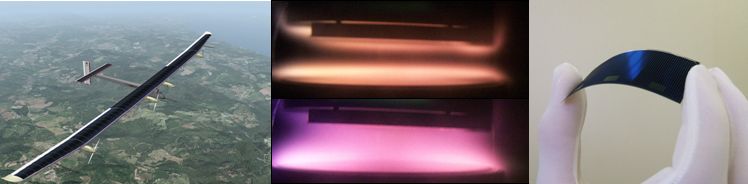
It is also active as a consultant for various companies. The Lab acts as an expert for the development and selection of solar cells for the Solar-impulse project.
Current research topics of the laboratory include
- Surface passivation and heterojunction structure (a-Si/c-Si) for the high efficiency cristalline Silicon cells
- Novel passivating contact structures for crystalline silicon solar cells
- Perovskite / silicon heterojunction tandem cells
- Amorphous and microcrystalline thin-film silicon layers and application to various devices
- Optimization of thin-film deposition processes (PE-CVD and LP-CVD)
- Transparent conductive oxides for electronic applications
- Electronic properties and growth of nanostructured materials
- Electronic thin films for application in particle or X-Ray detectors, and in flat screen displays; specialized applications of thin-film light sensors
- Packaging and reliability of PV-modules
- PV integration into bulding and vehicles
- PV energy systems