Hybrid NANO-CMOS
| Strained gate-all-around deeply scaled Si nanowire MOSFETs
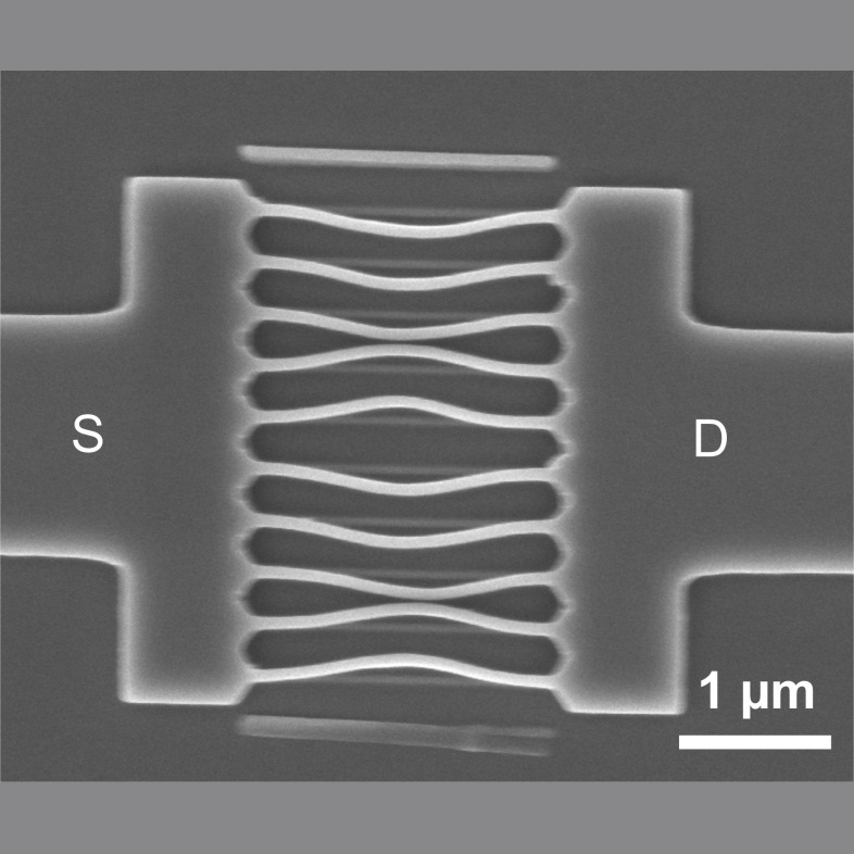
Development of a top-down Si nanowire platform on a SOI substrate to make dense array of gate-all-around Si nanowires with scalable NW cross-section down to 4 nm. High level of local uniaxial stress (both tensile and compressive) can be simply integrated to this platform using e.g. metal-gate strain and local oxidation to improve the carrier mobility. Transport analysis in such 1DEG architectures is being supported by extensive 3D TCAD device simulations. Work of Mohammad Najmzadeh
|
| FinFET mechanical resonator
Work of Sebastian Bartsch |
| Multi-gate buckled self-aligned dual Si nanowires on bulk Si
Formation of buckled two sub-100 nm cross-sectional Si NWs connected with a sub-10 nm thin Si bridge using 0.8 µm optical lithography, hard mask/spacer and local oxidation of a Si Fin on bulk Si substrate. The higher oxidation rate for the Si side-walls wrt. the top (100) surface and built-in stress in the growing oxide layer during oxidation yields two Si cores without pre-shape engineering e.g. scalloping. The thin Si bridge is being consumed during the gate stack step, resulting multi-gate self-aligned dual Si nanowire MOSFETs. Work of Mohammad Najmzadeh
|
| Nanowire Sensor Array
Work of Elizabeth Buitrago |
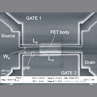 SEM micrograph of a very-high frequency FinFET mechanical resonator. The n-type enhancement mode FET is integrated in the centre of the beam. The in-plane motion at resonance modulates the 2-DEG in the channel of the FET, allowing sensitive nanomechanical motion detection, on-chip and at room temperature.
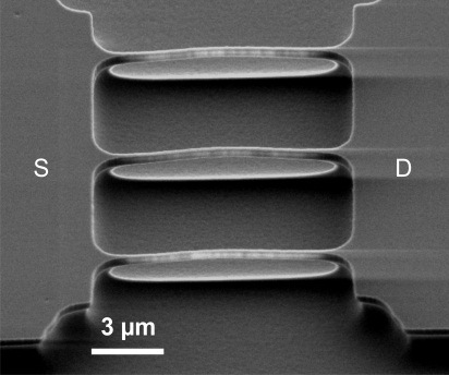
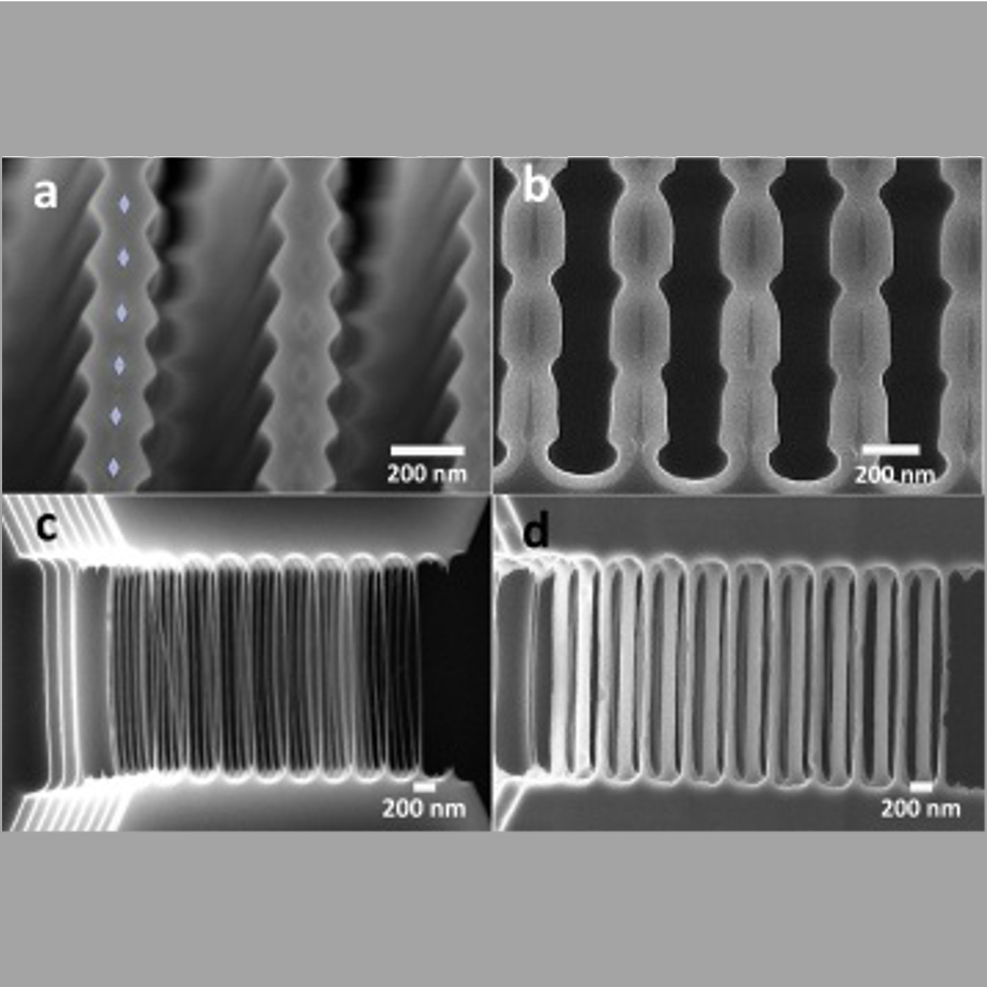 High density (7-10 NW/μm) Si-NW arrays of up to 16 nanowires vertically stacked with diameter widths below 20 nm have been successfully fabricated to create highly sensitive 3D FETs for biosensing applications. In order to take advantage of the increased sensing surface area that nanoscale 3D devices offer and improve the mechanical characteristics of the suspended sensing channels, vertically stacked Fin-type structures are also being investigated. The vertical stacking allows for higher utilization of the bulk Si with increasing output currents as the number of channels increases. a) Cross section view nanowire formation after oxidation, b) top-side view of vertically stacked NW array, c) fin definition after oxidation, d) suspended vertically stacked fin array.
 Hybrid (MEMS/NEMS)-CMOS
| Ferroelectric Tunnel FETs
Work of Livio Lattanzio |
| Flexible Radios
Work of Nenad Cvetkovic |
| NEM Logic switch
Work of Maneesha Rupakula, Antonios Bazigos |
| Organic Diode/Capacitor rectifier
Work of Nenad Cvetkovic
|
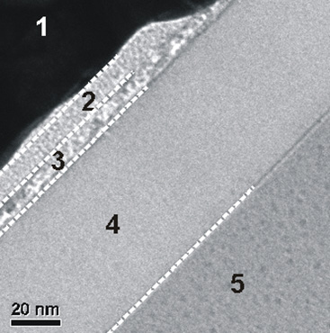 Fabricated Ferroelectric Tunnel FETs on thin film SOI substrates with a SiO2/Al2O3/P(VDF-TrFE) gate stack. The high resolution TEM micrograph shows the cross-section of the fabricated gate stack: (1) Au, (2) P(VDF-TrFE), (3) Al2O3 + pedestal SiO2, (4) Si and (5) buried oxide (BOX).
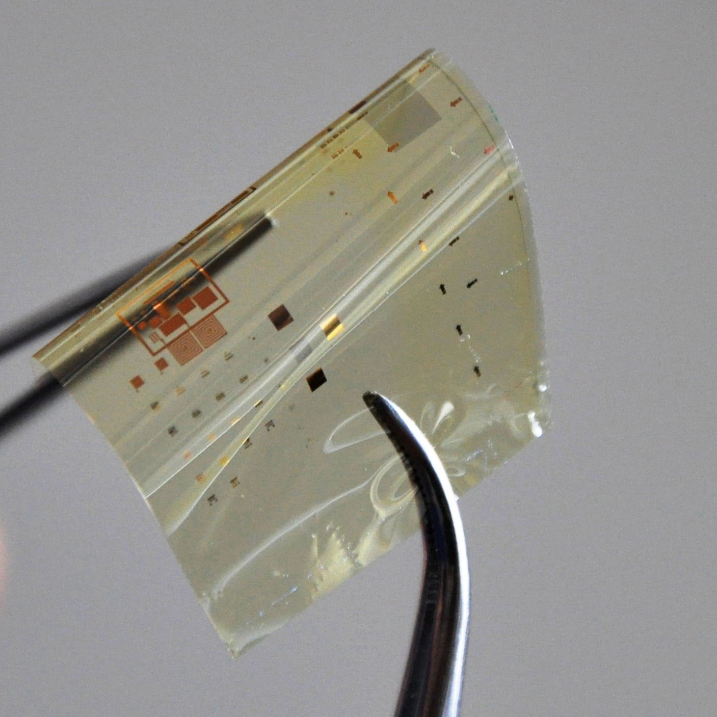 Microphotograph of OTFT devices on a flexible substrate once detached of a carrier Si-wafer; also shown are other passive and test devices (high-k capacitors and inductors) as well as small test circuits.
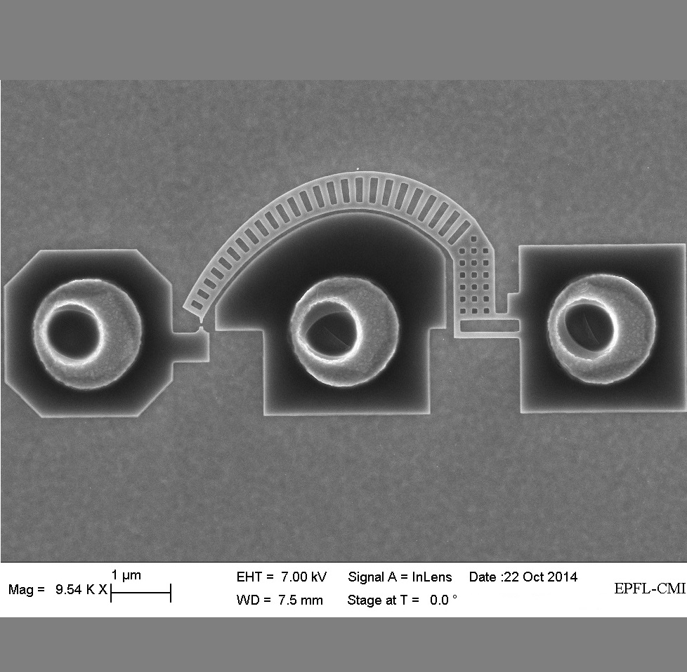 Fabrication of NEM Logic switch. SEM taken after the e-beam writing, where the cantilever with its tip, the gate and the drain/contact electrode are drawn. Critical dimension is 30nm and the gap between the gate and the cantilever is 60nm. The inclined cantilever design also prevents the beam landing on the gate due to the different angles of motion of the drain electrode and the beam. The relay is fabricated using a sacrificial layer, which ensures precise control of the air gap, with uniformity throughout the length of the beam. It also makes possible air gaps smaller than the lithographically defined limit, which in turn allows precise control of the electric fields and reduced footprints. Nano-electro-mechanical (NEM) relays have the advantage of essentially zero “off” current, and therefore has been the subject of much research to understand their potential in building logic circuits with the promise of order of magnitude improvements in energy efficiency. [
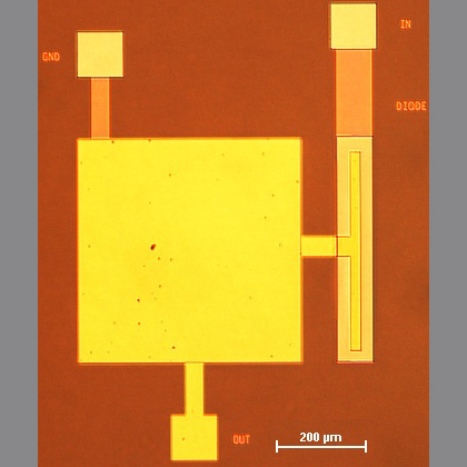 Microphotograph of Organic Diode/Capacitor rectifier fabricated on flexible substrate. The surface of Metal-Insulator-Metal capacitor (Al – 65 nm, HfO2 – 50 nm – Au – 120 nm) is 500