Ultrafast Electron Diffraction
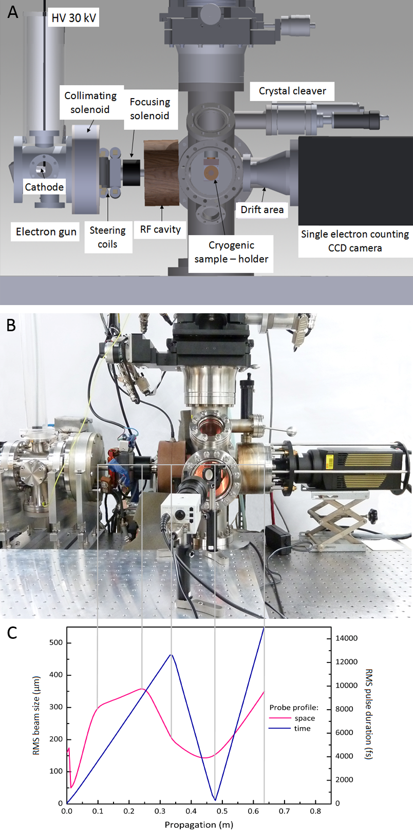 Ultrafast Electron Diffraction (UED) is a powerful method to investigate the structural dynamics of molecules and materials. Femtosecond (fs) electron bunches are used to obtain diffraction images of a specimen upon photo-excitation by a temporally delayed light pulse. The high cross-section of electrons makes it a very flexible tool for the study of light elements, monolayers and surfaces; at the same time, electrons can travel down to few nanometers (nm) and structural information from the bulk can also be retrieved. We have designed and implemented a flexible beamline for fs electron diffraction experiments in transmission or reflection geometry. By the use of a radiofrequency (RF) compression cavity synchronized to our laser system, in combination with a set of electron optics, we can control the beam properties in terms of charge per pulse, transverse spotsize on the sample and temporal duration of the bunches. Control of the sample temperature is obtained via a liquid helium flow-cryostat operating in the range between 1.8 K and 300 K. The whole beamline is designed to reach a vacuum around 10−10 mbar, and standard surface preparation tools such as a crystal cleaver and a tool for mechanical scraping are mounted on a removable feedthrough. The characterization of the system was performed via a light-electrons cross-correlation experiment and we obtained an overall temporal resolution around 300 fs for bunches containing up to 105 electrons at a repetition rate of 20 kHz.
http://www.sciencedirect.com/science/article/pii/S0168900212007334
![]()
Ultrafast Electron Microscopy
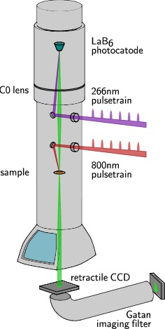
The microscope, constructed by Integrated Dynamic Electron Solutions (IDES), is a variant of the Dynamic Transmission Electron Microscope developed at Lawrence Livermore National Laboratory capable of probing photoinitiated processes in materials on femtosecond timescales with 2 Ångström resolution.
Ultrafast temporal resolution is achieved by generating a photoelectron probe using 266 nm laser pulses that are optically delayed relative to infrared pump pulses hitting the sample. To meet the energy, duration and repetition rate requirements we use a prototype laser system from KMLabs that delivers 50 fs pulses at a tunable repetition rate, single-shot to 1 MHz, with an energy of 1.57 eV per photon and an average power of 3 W.
The microscope is a modified JEOL JEM-2100 TEM equipped with IDES constructed laser port and C0 lens sections that enable two pulsed laser beams to enter the column; an ultraviolet beam to illuminate the LaB6 cathode, generating electron pulses, and an infrared beam to stimulate excitations in the sample.
In stroboscopic operation, to avoid space-charge effects and achieve femtosecond time resolution, every bunch of electrons should contain as few as one electron.
This poses limitations in terms of integration time however this is overcome by the high repetition rate of the laser system and the improved coupling into the condenser system provided by the C0 lens.
It is of capital importance to control the amount and spatial distribution of the charge photoemitted from the LaB6 tip.
To do this, the optical set-up is designed in order to match the UV spot size to the flat surface of the cathode (50 μm); this limits the emission area of the tip, without the relying on high Wehnelt bias settings.
The emitted electrons are then coupled in the column via an additional electromagnetic lens (C0 lens) located just below the electron gun. This solution allows optimal coupling of the photoemitted electrons to the condenser system.
High resolution images on a gold nanoparticle test sample have been collected to demonstrate that the modifications to the electron-optical system did not limit the spatial resolution of the microscope.
The energy spread of the electron beam has been also characterized via the postcolumn Gatan imaging filter. We notice here that the addition of the C0 lens allows us to efficiently couple electrons emitted from the filament and conserve the source brightness. Because the C0 lens allows much higher throughput, all the electrons emitted from the filament can be coupled to the standard TEM optics, producing currents as high as few microamps on the sample and detector. Thus lower filament heating currents can be used while maintaining reasonable signals on the detector, reducing the energy spread of the source and increasing spectroscopic energy resolution.
We measured the width of the zero loss peak using the GIF Quantum EELS spectrometer for different filament heating currents, Wehnelt bias voltage settings, and C0 lens voltage.
As is expected, using a lower filament heating current results in a narrower zero-loss peak. In addition, since the C0 lens improves coupling and allows high throughput, low Wehnelt bias voltages can be used to minimize the gun crossover and limit adverse Boersch effects that increase energy spread. We envision that with the C0 lens modification, low loss energy resolution of 0.4 eV can be achieved with currents >100 nA on the detector, a vast improvement over standard thermionic TEM technology. The C0 lens will also allow shorter integration times in stroboscopic pulse mode, minimizing drift and increasing both spatial and energy resolution.
Ultrafast Optical Spectroscopy
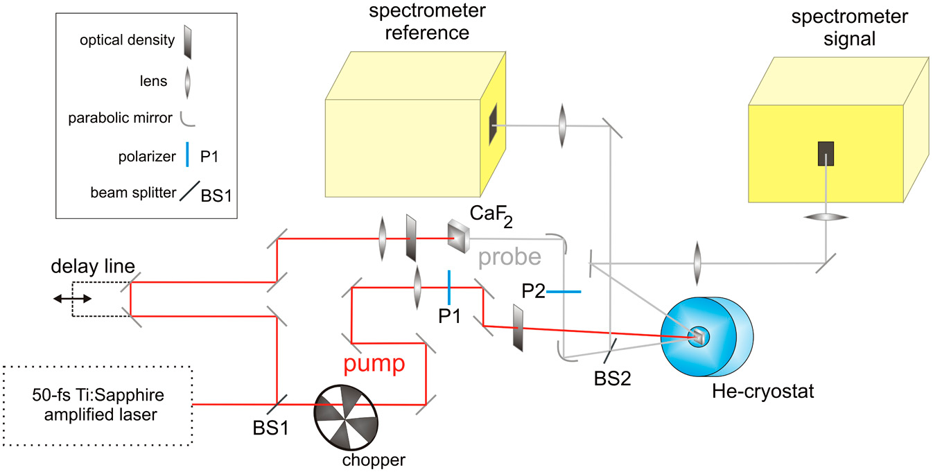
Our group features an optical broadband-probe reflectivity and transmission setup capable of measuring the transient behaviour in condensed matter on the femtosecond (fs) time scale. The system is laid out in pump-probe geometry as sketched in the illustration. It uses a 10 kHz sub-50 fs laser system providing pulse energies of up to 1.5 mJ at 800 nm. The broadband probe is produced in a calcium fluoride (CaF2) crystal that provides a continuous probing spectrum from about 400 nm to 750 nm. The pump beam can be varied in wavelength from the default 800 nm (1.55 eV) to 400 nm (3.1 eV) using a β-barium borate (BBO) crystal, or from 1200 nm into the mid-infrared up to 20,000 nm (0.062 meV) using an optical parametric amplifier. The setup is furthermore equipped with a low-vibration helium cryostat, allowing measurements at sample temperatures down to 10 K.
The setup provides us with a versatile tool to study electronic and phononic dynamics on a wide range of materials undervarying conditions. Since the optical data is obtained using a broadband probe, it is possible to extract the timely evolution of the complex optical constants (permittivity ε resp. conductivity σ) of the investigated sample by fitting a Drude-Lorentz model to the data. This model can further be used to perform a charge transfer analysis, providing information on the energetic redistribution of the electrons in the sample.
www.pnas.org/content/109/15/5603.full
Transient MOKE setup
Our group features a state-of-the-art transient magneto-optic Kerr effect (MOKE) setup. Using laser pulses of less than 50 fs width at a repetition rate of 5.2 MHz and a wavelength of 800 nm, this setup is capable of measuring the transient magnetization of a thin film or magnetic crystal with high precision. The setup can be used in combination with a low-vibration helium cryostat with a base temperature of 10 K. Measurements provide the timely evolution of the mangetic permeability μ. This information can be combined with results from the reflectivity setup of our group to obtain a complete picture of the electronic, lattice, and spin dynamics of a sample.