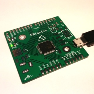
Before starting this tutorial, check the bottom side of your circuit board. you should find “Ver. 2.1.” on it. If it’s another version, make sure to use the adequate tutorial or talk to us, the committee, the instructions vary from version to version.
You’ll find all the components you need in the tray labelled as “pièces kit PRisme” in one of the drawer cabinets. Please only take a few components at the time, to avoid mixing them up and making a mess. If you think some components have run out or you’re not sure, inform us, we’ll restock them as soon as possible.
All the pieces you need for the kit PRisme are included in the price when you buy it.
Corresponding schematic
If you’re interested in learning to read schematics(the plans), you might want to have the PRismino schematic opened up. You can skip this, it’s not essential for the Kit Prism but certainly a usefull skill to have if you want to fix your own things one day for example. You can find the schematic on the Robopoly git account, or just use this link.
when a certain line is terminated by letters, it’s usually referred to as a flag. All flags with a common name are connect together in one single node. This gives as a significant improvement in the overview of the circuit. GND and VCC are very important flags corresponding to ground and “commun collector voltage” or simply the voltage you give your board. The big squares are so called ICs (integrated circuits). They are those little black squares that do all the thinking. Resistors are drawn as little squares marked with R, capacitors are usually represented by two parallel lines and marked with C.
Table of components
As a quick overview, here is the list of all the components you’ll need. make sure to get them all at once, it’s a terrible idea, you’ll end up wasting time trying to identify the components
| Component | Value |
| C1,C2 | 22 pF |
| C3 | 1 uF |
| C4, C5 | 100 nF |
| C6 | 10 uF |
| R1, R2 | 1 kΩ |
| R3, R4 | 22 kΩ |
| R5 | 10 kΩ |
| LED, PWR | LED 0805 |
| Component | Quantity |
| 8 pin female connector short | 2 |
| 6 pin female connector short | 2 |
| 2×3 male connectors | 1 |
| push button | 1 |
| 16MHz Oscillator | 1 |
Assembly guide
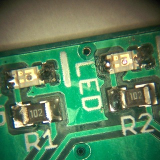
Step 1: Solder R1 and R2
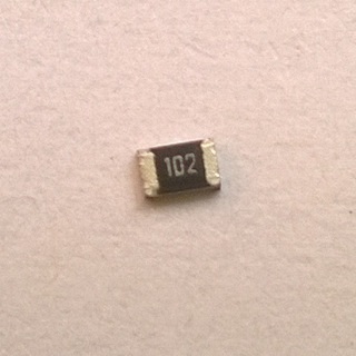
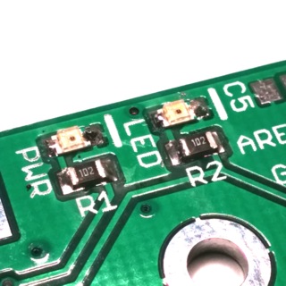
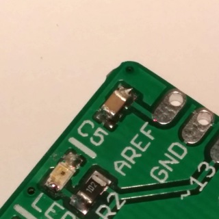
First you’ll need to get R1 and R2. Both are marked with the value 102. Resistors are usually labelled with a 3 digit number abc for which the corresponding resistance can be computed with the formula ab*10^c. For R1 and R2, 102 equals to 10*10^2 Ω or simply 1 kΩ. Start off by Soldering R1 and R2 in the places indicated on the PCB. The orientation of the components is not relevant, since they are both resistors. Resistors serve the purpose of restricting the current flow. as you can see they are both placed next to an Led. Restricting the current flow saves the Led from blowing out.
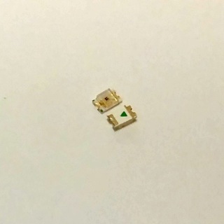
Step 2: Solder the LEDs
Now get two LEDs and solder them in place at the LED and PWR mark. Be aware of the sense you solder them in! If you flip the component over you’ll see either a dot on one end of the LED or an arrow. In the case of a dot, orient the dot towards the white line on the PCB or point the arrow towards this white line
Step 3: Testing what you’ve done so far
Plug the USB cable in and connect it to your computer. Your computer should deliver the energy to light up the PWR led (PWR = power, it means your board is recieving the power). If this is the case, you can move on, you’ve done good so far. The other LED is not supposed to light up. If the LED is not lighting up, check your soldering joints and the direction of your LED.
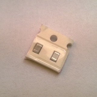
Step 4: Solder capacitors C1 and C2
Now we’ll solder on the capacitors C1 and C2. Make sure to check their value, if their value is not 22 pF your board might start acting strangely. The orientation of these components is not important. Capacitors serve the main function of smoothing out ripples in digital electronics. this means that even if the voltage at the entrance has some ripples, it gets smoothed out and our board can function “normally”. A good analogy for this is a garden hose. the water flowing out of it might vary in pressure and quantity. To stabilise it, we can add a paddling pool with a hole in it, so that the stream flowing out of that hole is constant in pressure and quantity, as long as there is enough water flowing into the pool. This is equivalent to the capacitors function
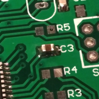
Step 5: Solder on capacitor C3
Do the same with the Capacitor C3. it’s value this time should be 1 uF
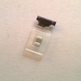
Step 6: Solder capacitors C4 and C5
And again for capacitors C4 and C5. Their value should be 100 nF.
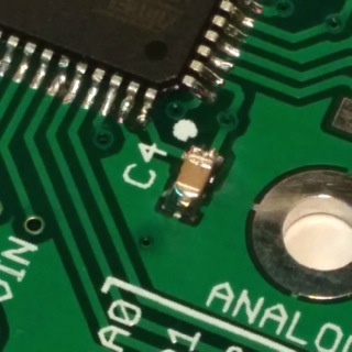
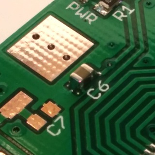
Step 7: Solder on C6
Solder capacitor C6 in its place. C6 has a value of 10 uF
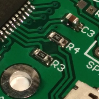
Step 8: Solder resistors R3 and R4
Solder resistors R3 and R4. As mentioned above, their value of 22 Ω is represented by the value 220. You may notice that they are placed on the line that goes to the USB port of the PCB. these resistors are connected in series to the data transmission lines of the USB. Understanding why takes quite a bit of theory. In real transmission lines we have to consider things like reflection of signals. To prevent this we can match the impedance of the line to the output impedance. impedance is a more generalised version of resistance.
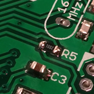
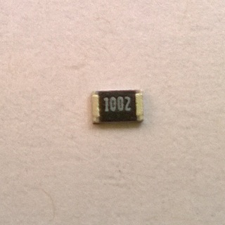
Step 9: Solder R5
Next you’ll have to solder R5 with a value of 1002 which is equivalent to 10 kΩ. this resistor is very important since it’s the reason why the reset button works. It’s a so called pull up resistor and it works by giving a reference voltage when the button is not pressed. every point in space has a certain potential, but the only way we can interact with this potential is by measuring it’s difference in space, so called Volts. measuring a difference implies that there has to be a reference voltage somewhere to which we compare the measurement to. It might be useful to look at the schematic and see that if the resistor wasn’t there, the line would go out and end in nothing when the button isn’t pressed. This state is usually referred to as floating and results in very random readings. Since we don’t want that, we reference the state of the button to VCC when the button isn’t pressed. If we connected the line directly to VCC without resistor, the resistance between VCC and GND would be virtually 0 when the button would be pressed, and there would be a very high current flow which would damage the board and also use a lot of energy.
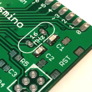
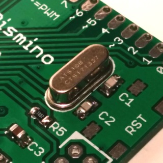
Step 10: Solder the Oscillator
This step is about the most important part of the circuit: the crystal oscillator. It generates a 16MHz oscillating signal. After soldering it in, flip the board and cut off it’s legs. For everything to be organised and synced up, there needs to be an oscillator serving as a clock, it is used as the reference time to execute operations and avoids implementing errors through the instability of real life components. Logic gates for example have a delay time before their output is updated. If we measured a value during this transition period, the output would be quite random once again.
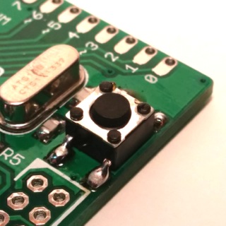
Step 11: solder the Push Button
Now solder the Push button on. The orientation doesn’t matter. It’s also known as the RST button, and resets the program.
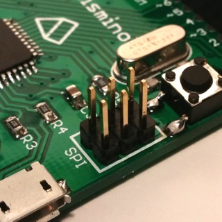
Step 12: Solder short pin connectors
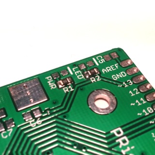
The next step is to solder the short connectors to the border of the board. Make sure they are as straight as possible when you solder them onto your board, and that they’re facing the same way as in the picture. the easiest way to achieve this is by starting by soldering one corner pin, aligning the connector, solder the opposite end pin and then the rest inbetween. This will be essential once we add the shield. You might have noticed that the order of this tutorial is not entirely random. In general it is good practice to start with the very small components then increasing in size and always working outwards. Imagine having to solder a resistor, now that the pins are in the way. What a world!
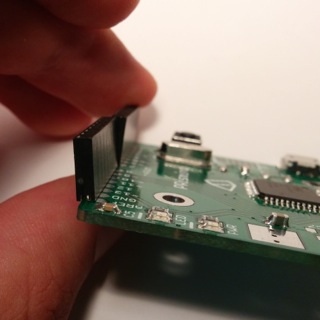
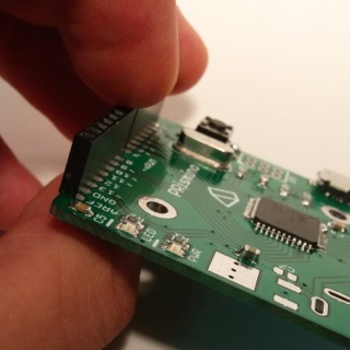
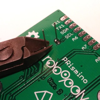
Step 13: Solder the SPI connector
This connector will also come into play with the shield later on, it will be doing the talking between the two boards and is also used to upload the very first program onto the board the so called bootloader. Make sure the long side of the legs are facing upwards. T
Step 14: loading the bootloader
Your board is almost ready. All microcontrollers are built in a very smart way (tap on the back for all the elecs(definitely not written by an elec)), where many many transistors are interconnected with fuses. Loading the bootloader means blowing out some of these fuses to create the desired logical behaviour. This means when the USB signal comes, the many many logic gates will translate the signal the desired way.
Loading the bootloader:
Find the Bootloader hidden somewhere in the Robopoly lab and follow this instructional video. After doing that, your board should be ready to receive its first program.
Programmation Guide
Step 1: downloading the Arduino IDE
You can choose to work on the Robopoly lab work station computer, but we strongly recommend downloading the arduino IDE onto your own computer. you can find it here.

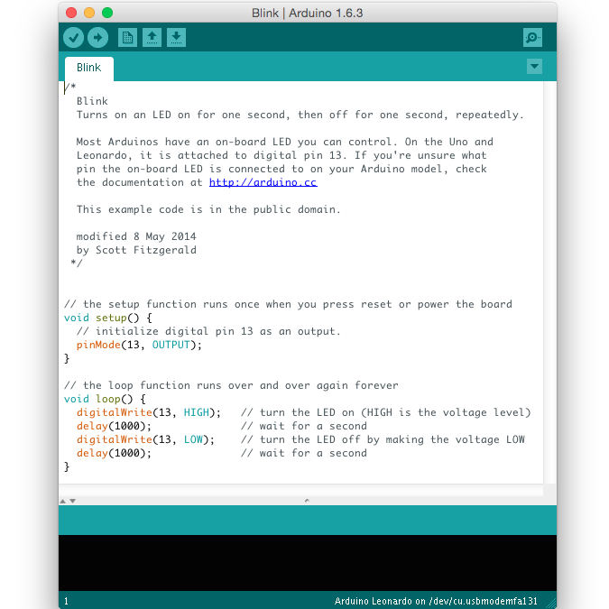
Step 2: testing the first program
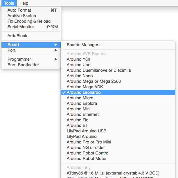
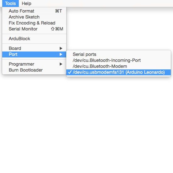
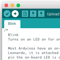
Open the Arduino IDE, go to: File > Examples > 1.Basics > Blink. this is an example code which will make the led on the board blink. Since there are many many microcontrollers with different Bootloaders it’s important to tell the program what board you’re connecting to it. To do that, go to: Tools > Board > Arduino Leonardo. Connect your board via USB to your computer. the last important part when programming an arduino is telling the computer what usb output the arduino is connected to. Got to Tools > Port, and select the right output. usually there should only be one output appearing, if multiple appear, brute force it, you should be fine and find it. you can also try changing the usb port you’re using
Step 3: upload the code to the arduino
Now you’re ready to compile the code and upload it to your ardunio via the 2 buttons on the top left corner of the IDE. Wait until the code is uploaded to the arduino, and the LED should start blinking. If you’re unfamiliar with prgoramming you can try changing the code to make the tics faster for example and reupload the code.
Next: Shield