Vertical power devices
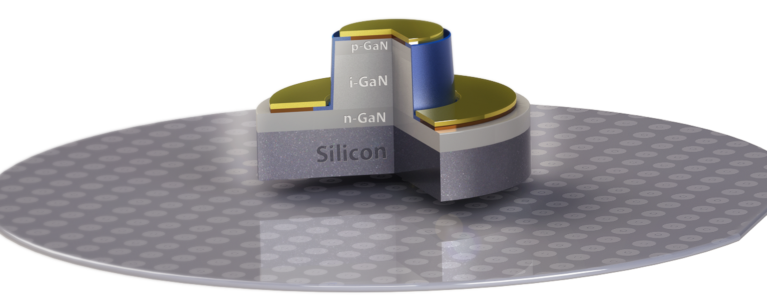
Our group has demonstrated a significant progress on vertical GaN power devices on cost-effective large-scale Silicon substrates, which could lead to the mass commercialization of vertical GaN devices due to the large-scale availability and mature fabrication technology of Silicon, compared to the less-available, expensive and small bulk GaN substrates.
This work has resulted in the demonstration of vertical GaN PiN diodes on 6” Silicon substrate with high breakdown voltage of 820 V and state-of-the-art figure of merit of 2.0 GW/cm2 , which at the time was 6-times larger than the highest value reported for GaN-on-Si vertical diodes. Following this work was the first demonstration of quasi-vertical GaN vertical power MOSFETs on 6” Silicon substrates, which were then monolithically integrated with Freewheeling Schottky Barrier Diodes.
Later we demonstrated the first fully-vertical GaN power MOSFETs on a 6-inch Si substrate. For the very first time, the feasibility of fully-vertical GaN MOSFETs on silicon substrate was shown, which opens huge opportunities for cost-effective vertical GaN devices. These results reveal a major step towards the realization of high performance GaN vertical power devices on cost-effective Si substrates.
Relevant publications:
- R. A. Khadar, C. Liu, L. Zhang, P. Xiang, K. Cheng, E. Matioli, “820 V GaN-on-Si Quasi-Vertical P-i-N Diodes with BFOM of 2.0 GW/cm2”, IEEE Electron Device Letters, 2018 (IEEE EDL editor’s pick)
- C. Liu, R. A. Khadar, E. Matioli, “GaN-on-Si Quasi-Vertical Power MOSFETs”, IEEE Electron Device Letters, 2018.
- C. Liu, R. A. Khadar, E. Matioli, “Vertical GaN-on-Si MOSFETs With Monolithically Integrated Freewheeling Schottky Barrier Diodes”, IEEE Electron Device Letters, 2018.
- R. A. Khadar, C. Liu, R. Soleimanzadeh, E. Matioli, “Fully-vertical GaN-on-Si power MOSFETs”, IEEE Electron Device Letters 2019.