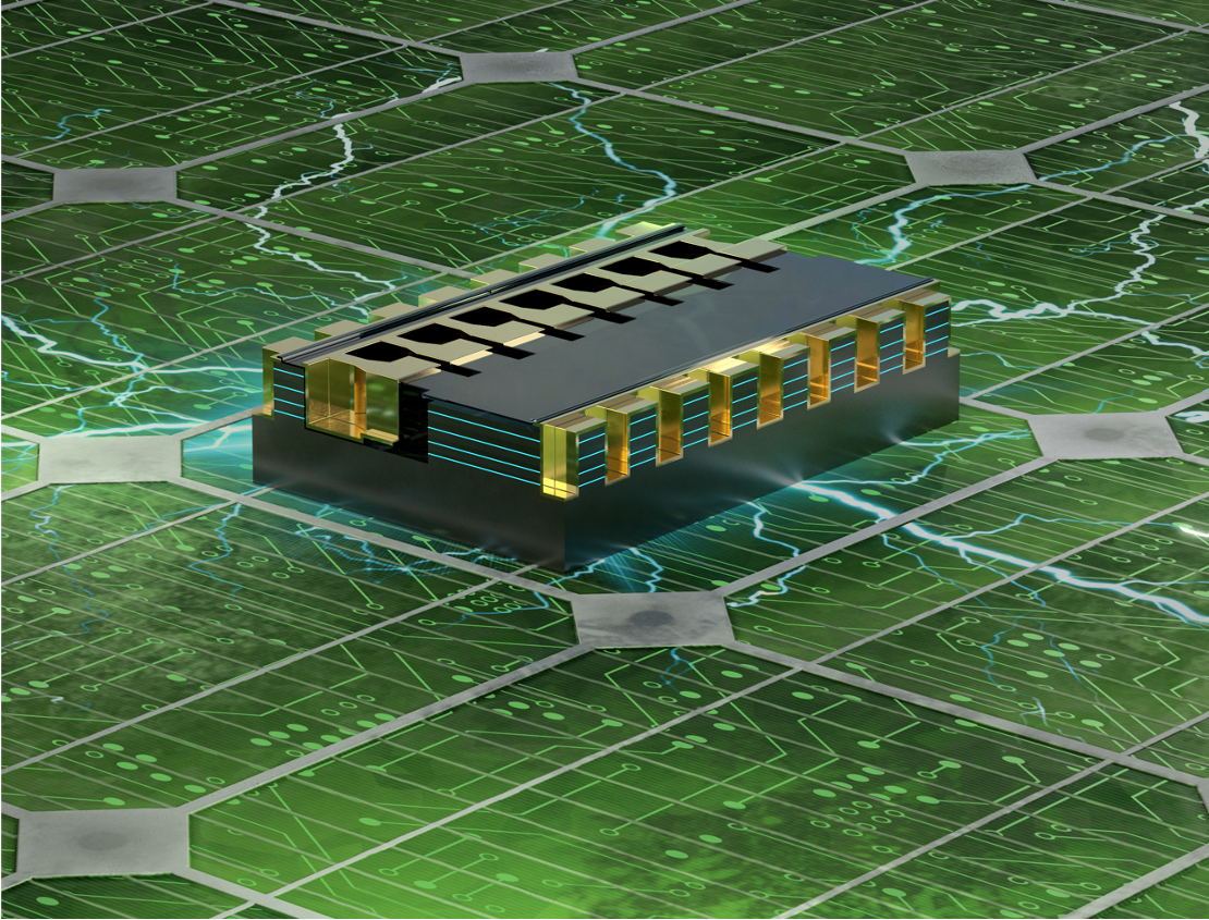
Lateral power electronic devices
The RON·Area product is a key figure of merit for power devices. A smaller RON·Area indicates lower conduction losses and more dies per wafer, for a given voltage rating. Therefore, it is an essential parameter for enhancing the efficiency and reducing the cost in power conversion. However, reducing RON· Area in GaN power devices is very challenging. RON is intrinsically determined by the electric conductivity of the 2DEG channel at the AlGaN/GaN interface, given by the product of its Ns and μ. Our group investigates novel devices and materials to break the traditional trade-offs in power devices.
For example, to drastically reduce on-resistance in power devices, we demonstrated a completely new concept of multi-channel power devices for future efficient power conversion. The multi-channel structure was judiciously designed to yield a small sheet-resistance of 80 Ω/sq., using only four 2DEG channels.
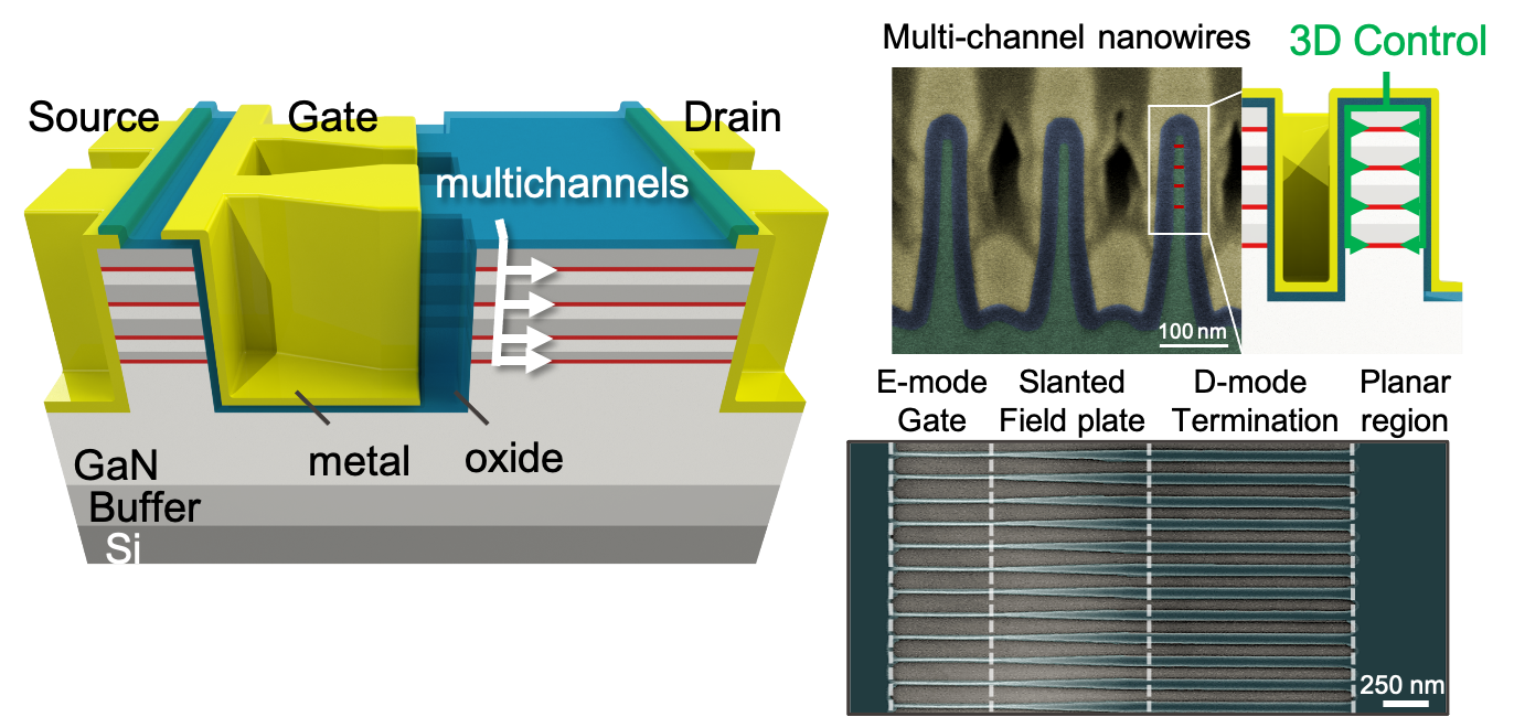
To address the limitation in breakdown voltage in lateral GaN power devices, due to their inhomogeneous electric field distribution, we proposed and demonstrated the new concept of slanted tri-gates designed to work as field plates and enhance the breakdown voltage in GaN power devices. Conventional field plates rely on a complex vertical design, whereas the proposed concept of slanted tri-gate relies on a lateral design, by gradually changing the width of the tri-gate wires, that is obtained with a single lithographic step.
Power devices exhibited ultra-low RON,sp of 0.46 mΩ·cm-2, enhancement-mode, breakdown voltages as high as 1300 V and a record figure-of-merit of 4.6 GW/cm2 for d-mode devices and 3.8 GW/cm2 for e-mode devices. These results significantly outperformed conventional single-channel devices and demonstrate the enormous potential of multi-channel devices for future efficient power solutions. This work was published in Nature Electronics 2021 (Mar2021).
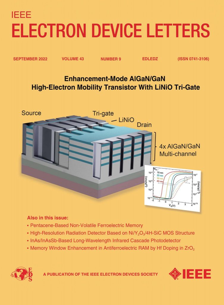
To reach enhancement-mode (e-mode) operation in multi-channel GaN transistors, we demonstrated conformally deposited p-type LiNiO over tri-gates to form a multi-channel junction gate structure. Compared to the normal MOS gate, the p-type LiNiO junction gate provides an additional depletion of the channels to yield a more positive VTH (1.2 V defined at 1 μA /mm).
Relevant publications:
-
L. Nela, J. Ma, C. Erine, P. Xiang, T.-H. Shen, V. Tileli, T. Wang, K. Cheng and E. Matioli, “Multi-channel nanowire devices for efficient power conversion” Nature Electronics, 2021
-
Wang, Y. Zong, L. Nela and E. Matioli, “Enhancement-Mode Multi-Channel AlGaN/GaN Transistors With LiNiO Junction Tri-Gate,” IEEE Electron Device Letters, 2022
- L Nela, H. K. Yildirim, C. Erine, R. Van Erp, P. Xiang, K. Cheng and E. Matioli, “Conformal Passivation of Multi-Channel GaN Power Transistors for Reduced Current Collapse”, IEEE Electron Device Letters, 2021
- J. Ma, C. Erine, M. Zhu, L Nela, P. Xiang, K. Cheng, E. Matioli “1200 V Multi-Channel Power Devices with 2.8 Ω·mm ON-Resistance”, 2019 IEEE International Electron Devices Meeting (IEDM), San Francisco, CA, USA, 2019.