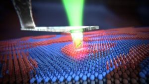
Quantum sensing is poised to revolutionise the future of sensing platforms. We want to contribute to this revolution by developing a very compact and highly sensitive magnetometer operating at room temperature, based on Nitrogen-Vacancy center spins in diamond. The high sensitivity offers the potential to do nanoscale protein sensing and the compact size makes the sensor applicable for small mobile platforms [1]. To achieve these goals, we will work in collaboration with the company LakeDiamond to establish in-situ nitrogen doping of CVD diamond during the growth, so that the resulting NV centers have long coherence times [2]. Moreover, we will explore growth along different crystal orientations in order to obtain self-aligned NV centers along a particular axis.
Characterizations capabilities at LQNO:
- CW-ODMR: Fluorescence is detected while applying an amplitude modulated microwave field to acquire continuous-wave ODMR spectra.
- Longitudinal spin relaxation (): It is the decay lifetime for NVs population initialized to a ground-state magnetic sublevel)
- (spin coherence time) using Hahn echo sequence
- (inhomogeneous spin dephasing time) using Ramsey sequence
- Cryogenic temperature measurement.
- Confocal mapping over 200x200x200um3 volume using either spectrometer or photodetector
[1] Lovchinsky, Igor, et al., Science 351.6275, 836-841 (2016).
[2] Kennedy, T. A., et al., Applied Physics Letters 83.20, 4190-4192 (2003).
Ongoing projects
Large area ultra-thin diamond membranes
Diamond has emerged as a promising platform for photonics and quantum technologies due to its ability to host color centers—impurities in the crystal lattice that create electronic states capable of absorbing and emitting visible light. These properties make diamond ideal for quantum sensing, imaging, and computing. Traditional bulk diamond photonic platforms rely on etching techniques like Focused Ion Beam (FIB) milling or Faraday cage angle etching to create free-standing waveguides, but these methods are complex and challenging to scale.
To enable large-scale fabrication, a Diamond-on-Insulator platform is desirable. Epitaxial growth offers a straightforward way to produce thin diamond films, but the harsh growth conditions often compromise crystal quality. Hybrid integration—where a diamond crystal is thinned and bonded to a carrier wafer—avoids this issue but involves lengthy, inhomogeneous processing and significant material loss.
An alternative approach, inspired by the SmartCut® technique used for silicon, is being developed in our group. This method involves implanting high-energy ions into a high-quality diamond crystal to create a damaged layer, which is then overgrown and subsequently etched away to release a thin membrane of controllable thickness and high crystalline quality. The process uses safe, controllable electrochemical etching to produce millimeter-sized membranes with uniform thickness. After strain relief and polishing (achieving ~1 nm roughness), the membrane is bonded to a carrier wafer, enabling scalable fabrication of photonic components with high consistency.
Additionally, membranes with high nitrogen-vacancy (NV) center density can be used for quantum sensing applications, such as nanoscale temperature measurements via zero-field spin splitting, or NV-enhanced IR absorption based magnetometry. This hybrid integration technique offers a more efficient and scalable solution for diamond-based photonic and quantum devices compared to traditional methods.


Absorption-based Quantum Sensing with NV centers in diamond photonic cavities
Diamond’s exceptional optical qualities make it a desirable platform for developing scalable quantum technologies. In particular, the ability to host color centers make it a potential choice for ambient condition quantum sensors. However, low photon collection efficiency and non-trivial microfabrication processes present significant challenges. Recent advances deviate its attention to infrared absorption optically detected magnetic resonance (IRA-ODMR) by monitoring the relative change in the infrared intensities upon a probe beam and microcavity-enhanced NV sensing techniques, nevertheless current approaches lack microscale spatial resolution. In this work, we bridge the gap by adiabatically transferring the mode from a tapered optical fiber to a tapered diamond waveguide, subsequently coupling the emitters to photonic crystal cavities (PhC) with small mode volumes. In principle, our technique converts more efficiently the probe photons into absorption signal thus enhance the SNR.
We fabricate the suspended PhC cavities from a single-crystal bulk diamond using the quasi-isotropic etching technique. It enables the possibility of ultra-thin devices by adjusting the undercut etching parameters. Our current results provide a proof-of-concept demonstration of integrated nanophotonic devices for potential NV optical coupling in IR domain. In the future, we are aiming to achieve a decent cooperativity and a step forward towards nanoscale spatial resolution with higher NV density samples.


A Superconductor-Spin Hybrid Quantum System for Quantum Simulation
Quantum simulation, the process of studying well-controlled model quantum systems can help us gain insight about complex quantum phenomena. Our goal is to develop an integrated hybrid quantum system for analog quantum simulation. We couple ensembles of NV centers to arrays of superconducting microwave resonators, and with this hybrid system we aim to develop new technologies useful for characterizing quantum technologies, and explore the physics of dissipative many-body systems.
In the weak coupling regime the NV centers can be used as microwave detectors to image the MW field amplitude and direction in the coupled cavity arrays. The freedom in designing the resonators and the couplings, combined with the small footprint allows us to study interesting MW photonic metamaterials exhibiting flat bands or topologically protected states that could have useful applications for quantum technologies.
By engineering strong coupling between the NV ensembles and the resonators we will be able study collective superradiant emission effects and the interaction of spin ensembles with artificial photonic environments.
Our study is carried out as a joint project between the Hybrid Quantum Circuits (HQC) group and the Laboratory of Quantum and Nano-Optics (LQNO). We intend to combine expertise in the design, fabrication, and characterization of superconducting quantum devices with know-how in quantum sensing using NV centers. We hope to gain new perspectives on both topics while developing a new hybrid spin-superconducting quantum simulation platform.


