One of the main research activities in our laboratory focuses on the investigation of the efficiency of InGaN/GaN quantum wells (QWs), the active region of visible light-emitting diodes (LEDs), which are nowadays widely used for solid-state lighting. Several defects severely impact the device performance, leading to a significant efficiency drop. For decades, dislocations have been considered as the main culprit but recently point defects have emerged to be highly critical. In particular, we have shown that defects lying at the surface of the high-temperature GaN buffer layer are incorporated in the InGaN/GaN QWs where they form non-radiative recombination centers [1]. To counteract this detrimental phenomenon, commercial LEDs feature an InGaN underlayer beneath the active region, which captures these defects and prevent them from reaching the active region [2]. In our laboratory, InGaN/GaN QWs are grown by metal-organic chemical vapor deposition (MOCVD). We employ a variety of advanced characterization techniques, such as photoluminescence, cathodoluminescence, atomic force microscopy, and X-ray diffraction, to study the formation, nature, and incorporation of these defects [3-5].
[1] C. Haller et al., Appl. Phys. Lett. 111, 262101 (2017).
[2] C. Haller et al., Appl. Phys. Lett. 113, 111106 (2018).
[3] Y. Chen et al., Appl. Phys. Lett. 118, 111102 (2021).
[4] T. F. K. Weatherley et al., Nano Lett. 21, 5217−5224 (2024).
[5] A. Toschi et al., APL Mater. 13, 031111 (2025).
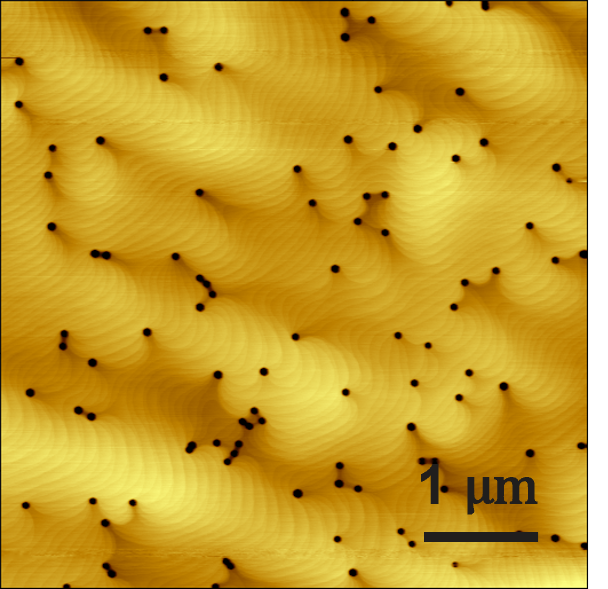
1. Atomic force microscopy image of a GaN epilayer grown on sapphire with an embedded single InGaN/GaN QW showing V-shape defect terminations.
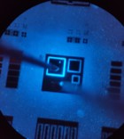
2. Optical micrograph of a blue light-emitting diode under forward bias.