


Motivation
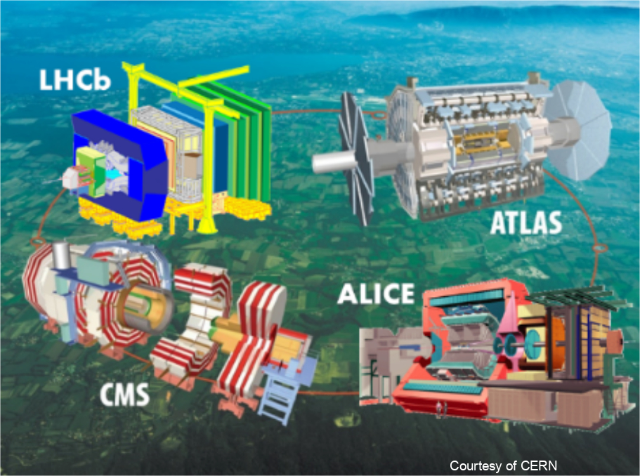
The Large Hadron Collider (LHC) at CERN is the world’s largest and most powerful scientific facility ever built. To promote the scientific progress, it will have a major upgrade in the 2020s for a ten-fold integrated luminosity. The electronics closest to collision points could thus experience an unprecedented radiation level of 1 Grad of total ionizing dose (TID) and 1016 neutrons/cm2 of hadron fluence over ten years of operation. With such a high integrated luminosity, the number of pile-up events can also reach up to 200, challenging the trigger and data acquisition systems. To ensure long-term reliable performance, the high-luminosity LHC (HL-LHC) will need highly improved particle detecting systems with higher bandwidth and a stronger radiation tolerance. Ultra-scaled gate oxides in MOSFETs tend to suppress the relevant charge trapping and reduce the susceptibility to TID. The aggressive downscaling of CMOS technologies also allows electronic devices to have a higher operation speed and extended circuit functionality. With the perspective of using ultra-scaled CMOS technologies for radiation-tolerant detectors, we are motivated to investigate the effects of ultrahigh TID levels on a commercial 28-nm bulk CMOS technology, in collaboration with CERN, INFN Padova and University of Padova, and INFN Milano-Bicocca and University of Milano-Bicocca.
Objectives
Since 45-nm technology node, a bilayer gate dielectric composed of a thin high-k material and an interfacial silicon dioxide has been introduced. In addition, the shallow trench isolation oxide is still in the order of 100 nm. Our objectives are to
- understand the effects of the radiation-induced charge buildup related to gate dielectrics and STI oxides on 28-nm bulk MOSFETs and
- accurately model the observed effects using BSIM6 or EKV MOSFET compact models that would enable designers to design circuits while accounting for the effects of total dose on device behaviors.
Results
Using CERN’s in-house 10-keV X-ray irradiation system, we have conducted most of the planned irradiation measurements on transistors of different types and geometries at different irradiation conditions. This 28-nm bulk CMOS process has been seen radiation tolerant and demonstrated its promising use in radiation-tolerant applications:
-
Most MOSFETs present a slight variation in subthreshold swing, threshold voltage, and channel mobility up to 1 Grad of TID, except narrow/long-channel MOSFETs being the worst case and nMOSFETs with a significant drain leakage current increase [1-3].
-
The free carrier mobility has been extracted using the Y-function. The results confirm the strong radiation tolerance of wide-channel MOSFETs that is attributed to the advanced gate stacks. Narrow-channel MOSFETs demonstrate a rather high mobility reduction that is attributed to the coulomb scattering of STI-related trapped charges [4].
-
Narrow/long-channel MOSFETs are sensitive to the radiation-induced positive charge trapping related to STI oxides. For a pMOSFET, STI-trapped positive charges prevent the formation of the p-channel along STI edges and cause a substantial loss in drain current [1]. For an nMOSFET, STI-trapped positive charges open two parasitic leakage paths along STI sidewalls, leading to a significant drain leakage current increase [5].
-
Similar results between diode and switched-on bias conditions imply a weak dependence of radiation-induced charge trapping on the horizontal electrical field. This might be due to the improved spacer processing or the higher energy barrier between SiO2 for spacers and HfO2 for the gate oxide [6].
To enable designers to account for radiation effects on circuit performance while designing circuits, we have been deriving physics-based models for the observed TID effects, targeting radiation-enhanced MOSFET compact models with a core charge-based physical model and models for non-ideal effects:
-
Towards the characterization of TID effects on analog parameters and transconductance efficiency of this 28-nm bulk CMOS technology, the simplified charge-based EKV MOSFET model has been used to describe large- and small-signal characteristics over a wide range of bias from weak to strong inversion [7].
-
The parasitic drain-to-source leakage current has been modeled as a function of TID with a semi-empirical physical model and the parallel parasitic device has been modeled as a charge-controlled gateless device using the simplified EKV MOSFET model [5, 8].
-
For a comprehensive description of TID effects, we have studied undoped symmetric long-channel double-gate MOSFETs with a charge-based physical model incorporating radiation-induced oxide- and interface-trapped charges [9].
-
Extending from the work on double-gate MOSFETs and introducing the simplified charge-based EKV MOSFET model, we have reached a model for characterizing electrical characteristics of 28-nm bulk MOSFETs with radiation-induced oxide- and interface-trapped charges as model parameters [10].
Publications
[1] C.-M. Zhang, F. Jazaeri, A. Pezzotta, C. Bruschini, G. Borghello, F. Faccio, S. Mattiazzo, A. Baschirotto, and C. Enz, “Characterization of Gigarad Total Ionizing Dose and Annealing Effects on 28-nm Bulk MOSFETs,” IEEE Transactions on Nuclear Science, vol. 64, pp. 2639-2647, 2017.
[2] C.-M. Zhang, F. Jazaeri, A. Pezzotta, C. Bruschini, G. Borghello, F. Faccio, S. Mattiazzo, A. Baschirotto, and C. Enz, “Gigarad Total Ionizing Dose and Post-irradiation Effects on 28 nm Bulk MOSFETs,” in 2016 IEEE Nuclear Science Symposium, Medical Imaging Conference and Room-Temperature Semiconductor Detector Workshop (NSS/MIC/RTSD), Strasbourg, France, 2016, pp. 1-4.
[3] A. Pezzotta*, C.-M. Zhang*, F. Jazaeri, C. Bruschini, G. Borghello, F. Faccio, S. Mattiazzo, A. Baschirotto, and C. Enz, “Impact of Gigarad Ionizing Dose on 28 nm Bulk MOSFETs for Future HL-LHC,” in 2016 46th European Solid-State Device Research Conference (ESSDERC), 2016, pp. 146-149.
[4] C.-M. Zhang, F. Jazaeri, G. Borghello, S. Mattiazzo, A. Baschirotto, and C. Enz, “Mobility Degradation of 28-nm Bulk MOSFETs Irradiated to Ultrahigh Total Ionizing Doses,” in 2018 IEEE International Conference on Integrated Circuits, Technologies and Applications (ICTA), 2018, pp. 162-163.
[5] C.-M. Zhang, F. Jazaeri, G. Borghello, F. Faccio, S. Mattiazzo, A. Baschirotto, et al., “Characterization and Modeling of Gigarad-TID-induced Drain Leakage Current in a 28 nm Bulk CMOS Technology,” presented at the 2018 IEEE Nuclear and Space Radiation Effects Conference (NSREC), Waikoloa, Hawaii, USA, 2018.
[6] C.-M. Zhang, F. Jazaeri, G. Borghello, S. Mattiazzo, A. Baschirotto, and C. Enz, “Bias Dependence of Total Ionizing Dose Effects on 28-nm Bulk MOSFETs,” in 2018 IEEE Nuclear Science Symposium, Medical Imaging Conference and Room-Temperature Semiconductor Detector Workshop (NSS/MIC/RTSD), Sydney, Australia, 2018.
[7] C.-M. Zhang, F. Jazaeri, A. Pezzotta, C. Bruschini, G. Borghello, S. Mattiazzo, A. Baschirotto, and C. Enz, “Total Ionizing Dose Effects on Analog Performance of 28 nm Bulk MOSFETs,” in 2017 47th European Solid-State Device Research Conference (ESSDERC), 2017, pp. 30-33.
[8] C.-M. Zhang, F. Jazaeri, G. Borghello, F. Faccio, S. Mattiazzo, A. Baschirotto, and C. Enz, “Characterization and Modeling of Gigarad-TID-induced Drain Leakage Current of 28-nm Bulk MOSFETs,” IEEE Transactions on Nuclear Science, vol. 66, pp. 38-47, 2019.
[9] F. Jazaeri, C.-M. Zhang, A. Pezzotta, and C. Enz, “Charge-Based Modeling of Radiation Damage in Symmetric Double-Gate MOSFETs,” IEEE Journal of the Electron Devices Society, vol. 6, pp. 85-94, 2018.
[10] C.-M. Zhang, F. Jazaeri, G. Borghello, F. Faccio, S. Mattiazzo, A. Baschirotto, and C. Enz, “Charge-based Modeling of Total-ionizing-dose Effects on Bulk MOSFETs in 28-nm Technology Node,” under internal review for IEEE Transactions on Electron Devices 2020.
