Additive Micro-Manufacturing for Plastic Micro-Electro-Mechanical-Systems
 |
 |
PI: Prof. Dr. Juergen Brugger
Project start: 1st October 2017
Project duration: 60 months
Summary
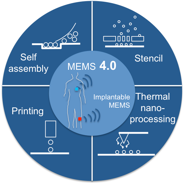
The manufacturing of silicon-based MEMS today is well advanced because the micro-electro-mechanical devices for automotive, domestic, health-care and consumer electronics can be fabricated with methods from IC industry. Polymer-based MEMS have a great potential for flexible electronics and biomedical applications, but to date, the techniques to engineer functional polymers into 3D microsystems, are still at their beginning because a coherent fabrication platform with the right tools and processes does not yet exist. The field could tremendously benefit from a coordinated effort in materials and manufacturing, in particular with a focus on biocompatible plastic materials. Additive manufacturing such as 3D printing and associated processing such as sintering has already started to transform traditional industry, but is not scalable much below a micrometer because the thermal processing is done in bulk or by lasers on surfaces. MEMS 4.0, in analogy with the industry 4.0 concept, aims to perform concerted research in additive manufacturing at the micro/nanoscale and associated key techniques. Using my expertise in MEMS and Nanotechnology, MEMS 4.0 will push the frontiers in new materials and new processing for MEMS by setting a focus on stencilling, printing, self-assembly and local thermal processing. This coherent processing framework will permit the use of delicate, soft, polymer materials to engineer the next generations of plastic MEMS. We are primarily targeting biodegradable implantable MEMS and permanently implantable glassy carbon MEMS. They are the most challenging to fabricate, but if successful, they also have an enormous impact for future wearables and implantables.
Progress
Along the main topics of this project, a brief overview of our recent research progress is listed in the following paragraphs:
1. Stenciling
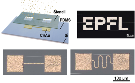
Microstencils have been fabricated by electron beam lithography (EBL) and deep-UV (DUV) lithography and benchmarked for various application purposes including for usage on biocompatible substrates. Metallic micro/nanostructures were stenciled onto biocompatible stretchable materials leading to the discovery of an original method to create large-scale liquid metal structures on stretchable biocompatible substrates. These liquid metal structures are investigated as versatile strain gauges for polymeric MEMS.
2. Printing
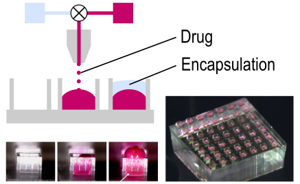
One of the challenges in drug delivery systems is to encapsulate the active substance in order to protect it from deterioration. We have developed an innovative approach for encapsulation of liquid drugs in a biocompatible micro-container to prevent evaporation of the liquid media (i.e. water). The encapsulation media and the drug are sequentially inkjet printed into a reusable template, followed by UV curing of the encapsulation layer.
3. Self-assembly
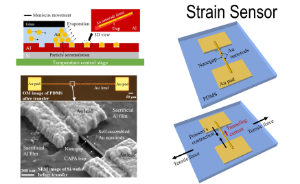
An electron-tunneling based strain sensor has been developed. The sensor has the following three characteristics: i) it is built on a stretchable biocompatible substrate poly(dimethylsiloxane) (PDMS) which makes it useful for wearable or implantable devices, ii) the strain-sensitive electrical signal is measured through two self-assembled gold nanorods separated by a distance of less than 2 nm, iii) a slick device design transforms the macroscopic strain of the PDMS into a sub-Ångström displacement which can be detected through a change in the electron-tunneling current.
4. Thermal nanoprocessing
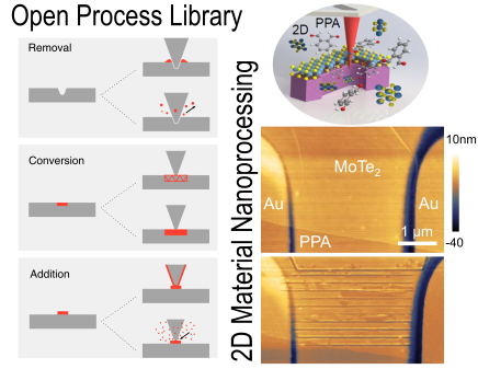
Thermal nanoprocessing of sub-100-nm structures through t-SPL is an emerging digital manufacturing technique. We have explored different ways to directly modify materials with a heated tip i.e. by annealing, melting or chemical modification. It was found that direct manipulation of 2D materials is an extremely compelling and versatile application of t-SPL. We have used t-SPL to locally cut 2D materials such as MoS2 or MoTe2 into arbitrary shapes [Liu et al. Adv. Mater. 2020, (accepted)]. A comprehensive thermal nano-processing library was published as an open-access review article.
5. Implantable biodegradable MEMS
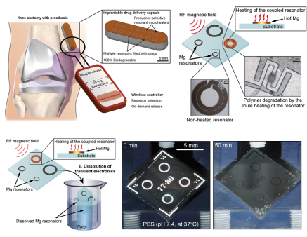
We fabricated implantable biodegradable capsules for wireless controlled drug release made from biodegradable elastomers poly(glycerol sebacate) (PGS) and poly(octamethylene maleate (anhydride) citrate) (POMaC) by an innovative imprinting process. The 10 x 10 x 20 mm3-sized drug containers accommodate up to six isolated reservoirs to be loaded separately with a drug. The capsules were covered with biodegradable membranes equipped with wirelessly powered microheaters that can be each addressed individually to release mL volumes of liquid drugs in each compartment separately. Wirelessly triggered release of the drug by breaking the membrane through heating was demonstrated, posing a significant step towards power receivers and microheaters for a variety of biodegradable implantable medical devices [M. Rüegg PhD Thesis EPFL 2020].
Publications
Microfabrication of lipids for drug delivery applications
Lausanne, EPFL, 2025.Laser-Induced Forward Transfer of SU-8 Microdisks as Carriers of Metallic Microdevices
Journal of Microelectromechanical Systems. 2024. DOI : 10.1109/JMEMS.2024.3487248.Performance Comparison of Shape Memory Polymer Structures Printed by Fused Deposition Modeling and Melt Electrowriting
Advanced Materials Technologies. 2024. DOI : 10.1002/admt.202400466.Development of core-shell lipid microneedles for sublingual delivery
2024.Near-Room-Temperature Detection of Aromatic Compounds with Inkjet-Printed Plasticized Polymer Composites
Acs Sensors. 2024. Vol. 9, num. 3, p. 1382 – 1390. DOI : 10.1021/acssensors.3c02406.Optical Ring Resonators in Sputtered Aluminum Nitride on Insulator for Integrated Photonic MEMS
2024. International Conference on Optical MEMS and Nanophotonics, San Sebastian, Spain, 2024-07-28 – 2024-08-01. DOI : 10.1109/OMN61224.2024.10685232.Liquid-in-a-MEMS: Encapsulation of Liquid in a Microcapsule by Inkjet Printing
2023.LIQUID-IN-A-MEMS: ENCAPSULATION OF LIQUID IN A MICROCAPSULE BY INKJET PRINTING
2023. 22nd International Conference on Solid-State Sensors, Actuators and Microsystems, Kyoto, Japan, 2023-06-25 – 2023-06-29.Laser-Induced Forward Transfer of Functional Microdevices
Lausanne, EPFL, 2023.Comparison of electrical and optical transduction modes of DNA-wrapped SWCNT nanosensors for the reversible detection of neurotransmitters.
Biosensors and Bioelectronics. 2022. Vol. 216, p. 114642. DOI : 10.1016/j.bios.2022.114642.Liquid encapsulated drug delivery device for acoustically-controlled release
2022.SU-8 cantilever with integrated pyrolyzed glass-like carbon piezoresistor
Microsystems & Nanoengineering. 2022. Vol. 8, num. 1, p. 22. DOI : 10.1038/s41378-022-00351-9.Precise Capillary‐Assisted Nanoparticle Assembly in Reusable Templates
Particle & Particle Systems Characterization. 2022. p. 1 – 8, 2100288. DOI : 10.1002/ppsc.202100288.Scalable fabrication of functional nanostructures on stretchable substrates by capillary-assisted particle assembly and adhesion lithography
Lausanne, EPFL, 2022.FABRICATION OF TRANSFERRED FLEXIBLE PMMA STENCIL LITHOGRAPHY
2022
SPONTANEOUS FORMATION AND PROGRAMMABLE ORIENTATION OF SURFACE WRINKLES ON THERMOSENSITIVE RESIST
2022
Multiscale 2D/3D microshaping and property tuning of polymer-derived SiCN ceramics
Journal of the European Ceramic Society. 2021. Vol. 42, num. 5, p. 1963 – 1970. DOI : 10.1016/j.jeurceramsoc.2021.12.044.Stretchable Conductors Fabricated by Stencil Lithography and Centrifugal Force-Assisted Patterning of Liquid Metal
ACS Applied Electronic Materials. 2021. Vol. 3, num. 12, p. 5423 – 5432. DOI : 10.1021/acsaelm.1c00884.High resolution meandering metal patterns enabled by nano-bridge stencil
47th international Conference on Micro and Nano Engineering (MNE2021), Turin, Italy, September 20-23, 2021.Edge-contact MoS2 transistors made by thermal scanning probe lithography
Micro and Nano Engineering Conference, Turin, Italy, September 20th – 23rd, 2021.Precise Capillary-Assisted Nanoparticle assembly in Reusable Templates
47th Micro and Nano Engineering Conference (MNE 2021), Turin, Italy, September 20-23, 2021.Printed Polymer Composite Sensors for Low-Power, Near Room-Temperature Detection and Classification of VOCS
2021. 34th International Conference on Micro Electro Mechanical Systems (IEEE MEMS 2021), Gainesville, FL, USA (virtual event), January 25-29, 2021. p. 274 – 277. DOI : 10.1109/MEMS51782.2021.9375208.Precision Surface Microtopography Regulates Cell Fate via Changes to Actomyosin Contractility and Nuclear Architecture
Advanced Science. 2021. Vol. 8, num. 6, p. 2003186. DOI : 10.1002/advs.202003186.A Glass-Like Carbon Mems Strain Sensor
2021. 21st International Conference on Solid-State Sensors, Actuators and Microsystems (Transducers), ELECTR NETWORK, Jun 20-25, 2021. p. 871 – 874. DOI : 10.1109/TRANSDUCERS50396.2021.9495726.Thermomechanical nanocutting and nanostraining of 2D materials
Heidelberg Instruments NanoFrazor Webinar series, 2021-02-09.Inkjet-printed polymer composites for the detection of volatile organic compounds
Lausanne, EPFL, 2021.Hierarchical Micromold Structuring via 2PP Micro-Stereolithography
2021.Electrochemical performance of polymer-derived SiOC and SiTiOC ceramic electrodes for artificial cardiac pacemaker applications
Ceramics International. 2020. Vol. 47, num. 6, p. 7593 – 7601. DOI : 10.1016/j.ceramint.2020.11.098.Thermomechanical Nanostraining of Two-Dimensional Materials
Nano Letters. 2020. Vol. 20, num. 11, p. 8250 – 8257. DOI : 10.1021/acs.nanolett.0c03358.On the effect of linear feedback and parametric pumping on a resonator’s frequency stability
New Journal Of Physics. 2020. Vol. 22, num. 9, p. 093049. DOI : 10.1088/1367-2630/abb1dd.Cracks, porosity and microstructure of Ti modified polymer-derived SiOC revealed by absorption-, XRD- and XRF-contrast 2D and 3D imaging
Acta Materialia. 2020. Vol. 198, p. 134 – 144. DOI : 10.1016/j.actamat.2020.07.067.Thermal and pH Sensitive Composite Membrane for On-Demand Drug Delivery by Applying an Alternating Magnetic Field
Advanced Materials Interfaces. 2020. Vol. 7, num. 17, p. 2000733. DOI : 10.1002/admi.202000733.Thermomechanical Nanocutting of 2D Materials
Advanced Materials. 2020. p. 2001232. DOI : 10.1002/adma.202001232.In Vitro Cytocompatibility Assessment of Ti-Modified, Silicon-oxycarbide-Based, Polymer-Derived, Ceramic-Implantable Electrodes under Pacing Conditions
ACS Applied Materials & Interfaces. 2020. Vol. 12, num. 15, p. 17244 – 17253. DOI : 10.1021/acsami.0c01465.Thermal scanning probe lithography-a review
Microsystems & Nanoengineering. 2020. Vol. 6, num. 1, p. 21. DOI : 10.1038/s41378-019-0124-8.Biodegradable Wireless Microheaters for Transient Biomedical Implants
NanoBioTech-Montreux, Montreux, Switzerland, November 20, 2019.Phase masks for electron microscopy fabricated by thermal scanning probe lithography
Micron. 2019. Vol. 127, p. 102753. DOI : 10.1016/j.micron.2019.102753.A 3D Microscaffold Cochlear Electrode Array for Steroid Elution
Advanced Healthcare Materials. 2019. p. 1900379. DOI : 10.1002/adhm.201900379.Harnessing Poisson Effect to Realize Tunable Tunneling Nanogap Electrodes on PDMS Substrates for Strain Sensing
2019. 20th International Conference on Solid-State Sensors, Actuators and Microsystems & Eurosensors XXXIII (TRANSDUCERS & EUROSENSORS XXXIII), Berlin, Germany, June 23-27, 2019. p. 2368 – 2371. DOI : 10.1109/TRANSDUCERS.2019.8808819.Liquid Assembly of Floating Nanomaterial Sheets for Transparent Electronics
Advanced Materials Technologies. 2019. p. 1900398. DOI : 10.1002/admt.201900398.Biodegradable Frequency‐Selective Magnesium Radio‐Frequency Microresonators for Transient Biomedical Implants
Advanced Functional Materials. 2019. Vol. 29, num. 39, p. 1903051. DOI : 10.1002/adfm.201903051.Novel Wearable Triboelectric Generator based on a Hybrid Mix of Carbon Nanotube and Natural Polymer
MEMS, Seoul, Korea,Wearable Triboelectric Generator based on a Hybrid Mix of Carbon Nanotube and Polymer Layers
2019. 18th International Conference on Micro and Nanotechnology for Power Generation and Energy Conversion Applications, Daytona Beach, FL, Dec 04-07, 2018. DOI : 10.1088/1742-6596/1407/1/012047.Combination of thermal scanning probe lithography and ion etching to fabricate 3D silicon nanopatterns with extremely smooth surface
Microelectronic Engineering. 2018. Vol. 193, p. 23 – 27. DOI : 10.1016/j.mee.2018.02.012.3D printed microchannels for sub-nL NMR spectroscopy
PLOS ONE. 2018. Vol. 13, num. 5, p. e0192780. DOI : 10.1371/journal.pone.0192780.Bioresorbable Frequency-Selective Magnesium Microresonators Fabricated by Ion Beam Etching
Microtechnologies in Medicine and Biology, Monterey, USA, 26-28 March 2018.PZE-transduced Suspended Microchannel Resonators for sensing applications
Lausanne, EPFL, 2018.Planar Optical Nanoantennas Resolve Cholesterol-Dependent Nanoscale Heterogeneities in the Plasma Membrane of Living Cells
Nano Letters. 2017. Vol. 17, num. 10, p. 6295 – 6302. DOI : 10.1021/acs.nanolett.7b02973.Self-assembly of micro/nanosystems across scales and interfaces
2017. 19th International Conference on Solid-State Sensors, Actuators and Microsystems (TRANSDUCERS 2017), Kaohsiung, Taiwan, June 18-22, 2017. p. 676 – 681. DOI : 10.1109/TRANSDUCERS.2017.7994139.Silk Fibroin as a Resist for Thermal Scanning Probe Lithography
43rd Micro and Nano Engineering Conference, Braga, Portugal, September 18-22, 2017.Preceramic Polymers as Precursor for implantable MEMS Applications
11th NAMIS International Autumn School “Micro & nano systems engineering: from fundamentals to industrial applications”, Freiburg, Germany, October 2-6, 2017.Penciling a triboelectric nanogenerator on paper for autonomous power MEMS applications
Nano Energy. 2017. Vol. 33, p. 393 – 401. DOI : 10.1016/j.nanoen.2017.01.053.Flexible fabric-based wearable solid-state supercapacitor
2017. IEEE 12th International Conference on Nano/Micro Engineered and Molecular Systems (NEMS), Los Angeles, CA, USA, April 9-12, 2017. p. 169 – 172. DOI : 10.1109/NEMS.2017.8016998.Penciling A Triboelectric Power Source On Paper
2016. 29th IEEE International Conference on Micro Electro Mechanical Systems (MEMS), Shanghai, PEOPLES R CHINA, JAN 24-28, 2016. p. 1169 – 1172. DOI : 10.1109/MEMSYS.2016.7421844.3D nanostructures fabricated by advanced stencil lithography
Nanoscale. 2016. Vol. 9, p. 4945 – 4950. DOI : 10.1039/C5NR08444J.A silk-fibroin-based transparent triboelectric generator suitable for autonomous sensor network
Nano Energy. 2016. Vol. 20, p. 37 – 47. DOI : 10.1016/j.nanoen.2015.11.036.Rapid carbon nanotubes suspension in organic solvents using organosilicon polymers
Journal of Colloid and Interface Science. 2016. Vol. 470, num. 15, p. 123 – 131. DOI : 10.1016/j.jcis.2016.02.050.Highly efficient and gentle trapping of single cells in large microfluidic arrays for time-lapse experiments
Biomicrofluidics – Fundamentals, Perspectives & Applications. 2016. Vol. 10, num. 1, p. 014120. DOI : 10.1063/1.4942457.High sensitivity field asymmetric ion mobility spectrometer
Lausanne, EPFL, 2016.Organic-inorganic-hybrid-polymer microlens arrays with tailored optical characteristics and multi-focal properties
Optics Express. 2015. Vol. 23, num. 19, p. 25365 – 25376. DOI : 10.1364/OE.23.025365.Development of Implantable Electrodes Based on Polymer Derived Ceramics
Lausanne, EPFL, 2015.Impedance sensing of DNA immobilization and hybridization by microfabricated alumina nanopore membranes
Sensors and Actuators B: Chemical. 2015. Vol. 216, p. 105 – 112. DOI : 10.1016/j.snb.2015.03.094.Resistless nanofabrication by stencil lithography: A review
Microelectronic Engineering. 2015. Vol. 132, p. 236 – 254. DOI : 10.1016/j.mee.2014.08.003.CNT and PDCs: A fruitful association? Study of a polycarbosilane–MWCNT composite
Journal of the European Ceramic Society. 2015. Vol. 35, num. 8, p. 2215 – 2224. DOI : 10.1016/j.jeurceramsoc.2015.02.016.Composite hydrogel-loaded alumina membranes for nanofluidic molecular filtration
Journal of Membrane Science. 2015. Vol. 477, num. 1, p. 151 – 156. DOI : 10.1016/j.memsci.2014.12.023.On the micrometre precise mould filling of liquid polymer derived ceramic precursor for 300-µm-thick high aspect ratio ceramic MEMS
Ceramics International. 2015. Vol. 41, num. 1, p. 623 – 629. DOI : 10.1016/j.ceramint.2014.08.112.Three Dimensional Microstructures for Cell Culture with Engineered Stiffness and Geometry
Lausanne, EPFL, 2014.Inkjet Printing of High Aspect Ratio Superparamagnetic SU-8 Microstructures with Preferential Magnetic Directions
Micromachines. 2014. Vol. 5, p. 583 – 593. DOI : 10.3390/mi5030583.PDMS-based, magnetically actuated variable optical attenuators obtained by soft lithography and inkjet printing technologies
Sensors and Actuators A: Physical. 2014. Vol. 215, p. 30 – 35. DOI : 10.1016/j.sna.2014.01.021.Automated Real-Time Control of Fluidic Self-Assembly of Microparticles
2014. 2014 IEEE International Conference on Robotics and Automation (ICRA 2014), Hong Kong (China), May 31 – June 7, 2014. p. 5860 – 5865. DOI : 10.1109/ICRA.2014.6907721.Liquid-Filled Sealed Mems Capsules Fabricated By Fluidic Self-Assembly
2014. IEEE International Conference on Micro Electro Mechanical Systems (MEMS 2014), San Francisco (USA), January 26-30, 2014. p. 56 – 59. DOI : 10.1109/MEMSYS.2014.6765572.Three-dimensional polymeric microtiles for optically-tracked fluidic self-assembly
Microelectronic Engineering. 2014. Vol. 124, p. 1 – 7. DOI : 10.1016/j.mee.2014.04.017.Fabrication of HepG2 Cell Laden Collagen Microspheres using Inkjet Printing
Journal of the Korean Society for Precision Engineering. 2014. Vol. 31, num. 8, p. 743 – 747. DOI : 10.7736/KSPE.2014.31.8.743.Actuated MEMS and NEMS for cell force spectroscopy and gas sensing applications
Lausanne, EPFL, 2014.Influence of carbon enrichment on electrical conductivity and processing of polycarbosilane derived ceramic for MEMS applications
Journal of the European Ceramic Society. 2014. Vol. 34, num. 15, p. 3559 – 3570. DOI : 10.1016/j.jeurceramsoc.2014.06.002.Polymeric variable optical attenuators based on magnetic sensitive stimuli materials
Journal Of Micromechanics And Microengineering. 2014. Vol. 24, num. 12, p. 125008. DOI : 10.1088/0960-1317/24/12/125008.Single-Cell 3D Bio-Mems Environment With Engineered Geometry And Physiologically Relevant Stiffnesses
2014. 27th IEEE International Conference on Micro Electro Mechanical Systems (MEMS), San Francisco, CA, JAN 26-30, 2014. p. 177 – 180. DOI : 10.1109/MEMSYS.2014.6765603.Microdrop generation and deposition of ionic liquids
Journal Of Materials Research. 2014. Vol. 29, num. 17, p. 2100 – 2107. DOI : 10.1557/jmr.2014.162.Acousto-fluidic system assisting in-liquid self-assembly of microcomponents
Journal of Micromechanics and Microengineering. 2013. Vol. 23, num. 12, p. 125026. DOI : 10.1088/0960-1317/23/12/125026.Lateral capillary forces
Surface tension in microsystems; Springer, 2013. p. 45 – 69.Preface: Special Issue: Euromat 2011-European Congress and Exhibition on Advanced Materials and Processes: Symposium A53 MEMS/NEMS for Sensorial and Actorial Materials
Journal Of Intelligent Material Systems And Structures. 2013. Vol. 24, num. 18, p. 2171 – 2171. DOI : 10.1177/1045389X13507157.Surface tension-driven self-assembly
Surface tension in microsystems; Berlin Heidelberg: Springer, 2013. p. 227 – 253.Reconfigurable MEMS modules for 2D (self-)assembly
2013.High-resolution 1D moirés as counterfeit security features
Light: Science & Applications. 2013. Vol. 2, num. 7, p. e86. DOI : 10.1038/lsa.2013.42.Fluid-mediated self-assembly of MEMS micro-capsules for liquid encapsulation and release
Lausanne, EPFL, 2013.Resistless Fabrication of Nanoimprint Lithography (NIL) Stamps Using Nano-Stencil Lithography
Micromachines. 2013. Vol. 4, p. 370 – 377. DOI : 10.3390/mi4040370.Simulation of Electrical Discharge Initiated by a Nanometer-Sized Probe in Atmospheric Conditions
Plasma Science & Technology. 2013. Vol. 15, num. 9, p. 845. DOI : 10.1088/1009-0630/15/9/02.Fluid-mediated parallel self-assembly of polymeric micro-capsules for liquid encapsulation and release
Soft Matter. 2013. Vol. 9, p. 9931 – 9938. DOI : 10.1039/c3sm51923f.Polymeric hemispherical pico-liter micro cups fabricated by inkjet printing
2013. 2013 8th IEEE International Conference on Nano/Micro Engineered and Molecular Systems (NEMS), Suzhou, China, 7-10 04 2013. p. 1119 – 1122. DOI : 10.1109/NEMS.2013.6559918.Design iterations on Lego R – like MEMS bricks
2013.Integrated long-range thermal bimorph actuators for parallelizable bio-AFM applications
IEEE Sensors Journal. 2013. Vol. 13, num. 8, p. 2849 – 2856. DOI : 10.1109/JSEN.2013.2261293.In-liquid MEMS assembly by optical trapping
2013. 2013 IEEE 26th International Conference on Micro Electro Mechanical Systems (MEMS), Taipei, Taiwan, 20-24 01 2013. p. 78 – 81. DOI : 10.1109/MEMSYS.2013.6474181.Special Issue on Selected Papers From the 11th IEEE Sensors Conference 2012
Ieee Sensors Journal. 2013. Vol. 13, num. 8, p. 2809 – 2809. DOI : 10.1109/Jsen.2013.2268687.Fabrication & Characterization of Thermally Actuated MEMS
2012.Design, Modeling and Optimization of Stochastic Reactive Distributed Robotic Systems
Lausanne, EPFL, 2012.OPTIMIZATION OF THE PHOTOPOLYMERIZATION OF A POLYMER DERIVED CERAMIC
2012. 38th International Micro & Nano Engineering Conference, Toulouse, France, September 16-20, 2012.Hydrodynamic Trap for Directed Self-Assembly of MEMS
2012. The 7th Annual IEEE International Conference on Nano/Micro Engineered and Molecular Systems, Kyoto, JAPAN, March 5 – 8, 2012.Sub micrometer ceramic structures fabricated by molding a polymer-derived ceramic
2012. Micro- and Nano-Engineering (MNE) 2011, Berlin, Germany, September 19-23, 2011. p. 272 – 275. DOI : 10.1016/j.mee.2012.04.024.Effects of tensile stress on electrical parameters of thin film conductive wires fabricated on a flexible substrate using stencil lithography
Microelectronic Engineering. 2012. Vol. 98, p. 230 – 233. DOI : 10.1016/j.mee.2012.07.016.Directly fabricated multi-scale microlens arrays on a hydrophobic flat surface by a simple ink-jet printing technique
Journal of Materials Chemistry. 2012. Vol. 22, num. 7, p. 3053 – 3058. DOI : 10.1039/c2jm15576a.Biomimetic soft lithography on curved nanostructured surfaces
2012. September 19-23, Berlin, Germany, p. 269 – 271. DOI : 10.1016/j.mee.2012.03.013.Mechanical and tribological properties of polymer-derived Si/C/N sub-millimetre thick miniaturized components fabricated by direct casting
Journal of the European Ceramic Society. 2012. Vol. 32, num. 8, p. 1759 – 1767. DOI : 10.1016/j.jeurceramsoc.2012.01.007.Heterogeneous material micro-transfer by ink-jet print assisted mould filling
Microelectronic Engineering. 2012. Vol. 98, p. 619 – 622. DOI : 10.1016/j.mee.2012.04.025.Conductivity of SU-8 Thin Films through Atomic Force Microscopy Nano-Patterning
Advanced Functional Materials. 2012. Vol. 22, num. 7, p. 1482 – 1488. DOI : 10.1002/adfm.201102789.Fabrication of epoxy spherical microstructures by controlled drop-on-demand inkjet printing
Journal of Micromechanics and Microengineering. 2012. Vol. 22, num. 7, p. 074012. DOI : 10.1088/0960-1317/22/7/074012.Integrated long-range thermal bimorph actuators for parallelizable bio-AFM applications
2012. 11th IEEE Sensors Conference, Taipei, Taiwan, October 28-31, 2012. p. 789 – 792. DOI : 10.1109/ICSENS.2012.6411507.Inkjet printing for MEMS
Inkjet-based Micromanufacturing; Germany: Wiley-VCH, 2012. p. 331 – 346.CAFM investigations of filamentary conduction in Cu2O ReRAM devices fabricated using stencil lithography technique
Nanotechnology. 2012. Vol. 23, num. 49, p. 495707. DOI : 10.1088/0957-4484/23/49/495707.Containers assembled in fluid and corresponding production
US2012145572; WO2010122499; WO2010122499.
2011.Advances in Nanostenciling: resistless nanopatterning enables new applications
Swiss NanoConvention, Baden, Switzerland, May 18-19, 2011.Fabrication of polymeric micro structures by controlled drop on demand inkjet printing
2011. 22nd Micromechanics and Micro systems Europe Workshop, Toensberg, Norway, June 19-22, 2011. p. 97 – 100.Metallic Nanodot Arrays by Stencil Lithography for Plasmonic Biosensing Applications
ACS Nano. 2011. Vol. 5, num. 2, p. 844 – 853. DOI : 10.1021/nn1019253.Oxide nanocrystal based nanocomposites for fabricating photoplastic AFM probes
Nanoscale. 2011. Vol. 3, p. 4632 – 4639. DOI : 10.1039/c1nr10487j.Robust PECVD SiC membrane made for stencil lithography
Microelectronic Engineering. 2011. Vol. 88, p. 2790 – 2793. DOI : 10.1016/j.mee.2010.11.056.Hybrid polymer microlens arrays with high numerical apertures fabricated using simple ink-jet printing technique
Optical Materials Express. 2011. Vol. 1, num. 2, p. 259 – 269. DOI : 10.1364/OME.1.000259.SiN membranes with submicrometer hole arrays patterned by wafer-scale nanosphere lithography
Journal of Vacuum Science & Technology B. 2011. Vol. 29, num. 2, p. 021012/1 – 5. DOI : 10.1116/1.3554404.Inkjet printing of SU-8 for high-aspect ratio spherical polymeric microstructures
Swiss-eprint, Basel, Switzerland, December, 1-2, 2011.New inks for the direct drop-on-demand fabrication of polymer lenses
2011. 36th International Conference on Micro & Nano Engineering (MNE), Genoa, Italy, September 19-22, 2010. p. 2174 – 2179. DOI : 10.1016/j.mee.2010.12.004.Ultra-low power palladium-coated MEMS resonators for hydrogen detection under ambient conditions
2011. 16th International Conference on Solid-State Sensors, Actuators and Microsystems (TRANSDUCERS), Beijing, China, 5-9 June, 2011. p. 787 – 790. DOI : 10.1109/TRANSDUCERS.2011.5969266.Nanoelectromechanical systems (NEMS)
E-nano newsletter. 2011. Vol. 24, p. 37 – 59.High Throughput Nanofabrication of Silicon Nanowire and Carbon Nanotube Tips on AFM Probes by Stencil-Deposited Catalysts
Nano Letters. 2011. Vol. 11, num. 4, p. 1568 – 1574. DOI : 10.1021/nl104384b.The effects of channel length and film microstructure on the performance of pentacene transistors
Organic Electronics. 2011. Vol. 12, num. 2, p. 336 – 340. DOI : 10.1016/j.orgel.2010.12.004.100 mm dynamic stencils pattern sub-micrometre structures
Nanoscale. 2011. Vol. 3, num. 7, p. 2739. DOI : 10.1039/c1nr10083a.Reliable and Improved Nanoscale Stencil Lithography by Membrane Stabilization, Blurring and Clogging Corrections
IEEE Transactions on Nanotechnology. 2011. Vol. 10, num. 2, p. 352 – 357. DOI : 10.1109/TNANO.2010.2042724.Integrated MEMS actuation for force spectroscopy in liquid
Nano-Tera Annual Plenary Meeting, Bern, CH, May 12-13, 2011.Stencil Lithography and Inkjet Printing as New Tools for Life Sciences Research
Lausanne, EPFL, 2011.Organic Thin Film Transistors on Flexible Polyimide Substrates Fabricated by Full Wafer Stencil Lithography
Sensors and Actuators A: Physical. 2010. Vol. 162, num. 2, p. 155 – 159. DOI : 10.1016/j.sna.2010.04.016.Mechanically tuneable microoptical structure based on PDMS
Sensors and Actuators A: Physical. 2010. Vol. 162, num. 2, p. 260 – 266. DOI : 10.1016/j.sna.2010.02.025.Wafer-Scale Fabrication of Thin SiN Membranes and Au Films and Membranes with Arrays of Sub-um Holes Using Nanosphere Lithography
Lausanne, EPFL, 2010.Direct writing laser of high aspect ratio epoxy microstructures
Journal of Micromechanics and Microengineering. 2010. Vol. 21, num. 1, p. 017003. DOI : 10.1088/0960-1317/21/1/017003.Organic Pentacene Thin Film Transistors on Flexible Substrates Fabricated by Stencil Lithography
Lausanne, EPFL, 2010.Modeling Self-Assembly at All Scales
Nano-Tera.ch Annual Plenary Meeting, Bern, Switzerland, April 29, 2010.Large arrays of chemo-mechanical nanoswitches for ultralow-power hydrogen sensing
Journal of Micromechanics and Microengineering. 2010. Vol. 20, p. 105019. DOI : 10.1088/0960-1317/20/10/105019.Pd-functionalized MEMS resonator for hydrogen gas sensing at ambient pressure
7th International Workshop on Nanomechanical Cantilever Sensors, Banff, Canada., May 26-28, 2010.MAGNETIC NANOCRYSTAL MODIFIED EPOXY PHOTORESIST FOR MICROFABRICATION OF AFM PROBES
MEMSWAVES 2010 and MEMS, Italy, 2010.Very Large Scale Arrays of Chemo-Mechanical Nano-Switches for Ultralow Power Hydrogen Sensing
2010. 23rd International IEEE Conference on Micro Electro Mechanical Systems MEMS’2010, Hong Kong, 24-28 January, 2010. DOI : 10.1109/MEMSYS.2010.5442547.Sputtering of (001)AlN thin films: Control of polarity by a seed layer
Journal of Vacuum Science & Technology B: Microelectronics and Nanometer Structures. 2010. Vol. 28, num. 6, p. L61. DOI : 10.1116/1.3501117.Magnetic nanocrystal modified epoxy photoresist for microfabrication of AFM probes
2010. MEMSWAVES 2010 and MEMS, Italy, 2010. p. 580 – 584.Pd-functionalized MEMS resonator for hydrogen gas sensing
Nano-Tera Annual Plenary Meeting, Bern, Switzerland, April 29, 2010.Direct write laser at visible wavelength for patterning of high aspect ratio epoxy materials
2010. EIPBN- The 54th International Confrence on Electron, Ion, Photon Beam Technology and Nanofabrication, Anchorage, Alaska, USA, June 1-4, 2010.Direct Etching of High Aspect structures through a Stencil
2009. MEMS 2009, Sorrento, Italy, January 25-29, 2009. DOI : 10.1109/MEMSYS.2009.4805339.Nanomechanical mass sensor for monitoring deposition rates through confined apertures
The 4th Annual IEEE International Conference on Nano/Micro Engineered and Molecular Systems (NEMS), Shenzhen, China, January 5-8, 2009.Quick and Clean: Stencil Lithography for Wafer-Scale Fabrication of Superconducting Tunnel Junctions
IEEE Transactions on Applied Superconductivity. 2009. Vol. 19, num. 3, p. 242 – 244. DOI : 10.1109/TASC.2009.2019075.Nanomechanical Mass Sensor for Spatially Resolved Ultrasensitive Monitoring of Deposition Rates in Stencil Lithography
Small. 2009. Vol. 5, p. 176 – 180. DOI : 10.1002/smll.200990007.Drop-On-Demand Inkjet Printing of SU-8 Polymer
Micro and Nanosystems. 2009. Vol. 1, num. 1, p. 63 – 67. DOI : 10.2174/1876402910901010063.Longitudinal detection of ferromagnetic resonance using x-ray transmission measurements
Review of Scientific Instruments. 2009. Vol. 80, num. 12, p. 123902. DOI : 10.1063/1.3267192.Organic Thin Film Transistors on Flexible Polyimide Substrates Fabricated by Full Wafer Stencil Lithography
2009. XXIII Eurosensors Conference, Lausanne, Switzerland, September 6-9, 2009.. DOI : 10.1016/j.proche.2009.07.190.Stress and aging minimization in photoplastic AFM probes
Microelectronic Engineering. 2009. Vol. 86, num. 4-6, p. 1226 – 1229. DOI : 10.1016/j.mee.2008.12.033.Inkjet printing and high aspect ratio structuring for polymer-based micro and nano systems
Lausanne, EPFL, 2008.Inkjet printing of SU-8 for polymer-based MEMS: A case study for microlenses
21st IEEE International Conference on Micro Electro Mechanical Systems (MEMS 2008), Tucson, USA, 13-17 January, 2008.Full-wafer fabrication by nanostencil lithography of micro/nanomechanical mass sensors monolithically integrated with CMOS
Nanotechnology. 2008. Vol. 19, num. 30, p. 305302. DOI : 10.1088/0957-4484/19/30/305302.Magnetic Nanocrystals Modified Epoxy Photoresist for fabrication of NEMS and MEMS
2008. 34th International Conference on Micro and Nano Engineering (MNE’2008), Athens, Greece, September 15-18, 2008.Nanopatterned Self-Assembled Monolayers by Using Diblock Copolymer Micelles as Nanometer-Scale Adsorption and Etch Masks
Advanced Materials. 2008. Vol. 20, num. 10, p. 1962 – 1965. DOI : 10.1002/adma.200702005.Etching of sub-micrometer structures through Stencil
Microelectronic Engineering. 2008. Vol. 85, p. 1010 – 1014. DOI : 10.1016/j.mee.2007.12.068.Stress and aging minimization in photoplastic AFM probes
2008. 34th International Conference on Micro and Nano Engineering 2008 (MNE 2008), Athens, Greece, September 15-18, 2008. DOI : 10.1016/j.mee.2008.12.033.Reusability of nanostencils for the patterning of Aluminum nanostructures by selective wet etching
Microelectronic Engineering. 2008. Vol. 85, num. 5-6, p. 1237 – 1240. DOI : 10.1016/j.mee.2007.12.083.Dynamic stencil lithography on full wafer scale
Journal of Vacuum Science and Technology B. 2008. Vol. 26, p. 2054 – 2058. DOI : 10.1116/1.2987953.Stress and aging minimization in photoplastic AFM probes
34th International Conference on Micro and Nano Engineering 2008 (MNE 2008), Athens, Greece, September 15-18, 2008.Fabrication of Highly Ordered Vertical Nanogap Arrays and Networks on a Large Scale
34th International Conference on Micro- and Nano Engineering 2008 (MNE 2008), Athens, Greece, September 15-18, 2008.The gas flow rate increase obtained by an oscillating piezoelectric actuator on a micronozzle
Sensors and Actuators A: Physical. 2008. Vol. 144, p. 154 – 160. DOI : 10.1016/j.sna.2007.12.024.Research activities at LMIS1-EPFL
5th NAMIS International workshop, Freiburg, Germany, April 4th-5th, 2008.Compact CMOS current conveyor for integrated NEMS resonators
Iet Circuits Devices & Systems. 2008. Vol. 2, p. 317 – 323. DOI : 10.1049/iet-cds:20070320.Etching of sub-micrometer structures through Stencil
2008. 33rd International Conference on Micro- and Nano Engineering 2007 (MNE 2007), 23-26 Sept, 2007, Copenhagen, Denmark, Copenhagen, Denmark, 23-26 Sept, 2007. p. 1010 – 1014. DOI : 10.1016/j.mee.2007.12.068.Tunable, high aspect ratio pillars on diverse substrates using copolymer micelle lithography: an interesting platform for applications
Nanotechnology. 2008. Vol. 19, num. 28, p. 285301. DOI : 10.1088/0957-4484/19/28/285301.Mechanical stabilisation and design optimisation of masks for stencil lithography: Numerical approach and experimental validation
Microelectronic Engineering. 2008. Vol. 85, p. 2243 – 2249. DOI : 10.1016/j.mee.2008.07.009.Inkjet printing of SU-8 for polymer-based MEMS a case study for microlenses
2008. 21st IEEE International Conference on Micro Electro Mechanical Systems 2008, Tucson, Arizona, USA, Jan 13-17, 2008. p. 407 – 410. DOI : 10.1109/MEMSYS.2008.4443679.Highly Sensitive Si Cantilevers, with and without Magnetic Tip, for Magnetic Resonance Force Microscopy
14th International Conference on Solid-State Sensors, Actuators and Microsystems (Transducers ’07), Lyon, France, 10-14 June, 2007.Dry etching for the correction of gap-induced blurring and improved pattern resolution in nanostencil lithography
Journal of Microlithography, Microfabrication, and Microsystems. 2007. Vol. 6, p. 013005 – 1. DOI : 10.1117/1.2435273.Computational Design and Optimisation of Mechanically Reinforced Masks for Stencil Lithography
EuroSimE 2007, Thermal, Mechanical and Multiphysics Simulation and Experiments in Micro-Electronics and Micro-Systems,, London, UK, 15-18 April, 2007.Predicting mask distortion, clogging and pattern transfer for stencil lithography
Microelectronic Engineering. 2007. Vol. 81, num. 1, p. 42 – 53. DOI : 10.1016/j.mee.2006.08.003.An Epoxy Photoresist Modified by Luminescent Nanocrystals for the Fabrication of 3D High-Aspect-Ratio Microstructures
Advanced Functional Materials. 2007. Vol. 17, p. 2009 – 2017. DOI : 10.1002/adfm.200700098.Improved and new properties of resist materials by doping with nanoparticles and nanocrystals
Solutions for the Microsystems Technology Market (Microsys 2007 Congress), Berlin, Germany, 7- 8 March, 2007.Micropositioning and microscopic observation of individual picoliter-sized containers within SU-8 microchannels
Microfluidics and Nanofluidics. 2007. Vol. 3, num. 2, p. 189 – 194. DOI : 10.1007/s10404-006-0119-2.A Compact and Low-Power CMOS Circuit for Fully-Integrated NEMS Resonators
IEEE Transactions on Circuits and Systems II. 2007. Vol. 54, num. 5, p. 377 – 381. DOI : 10.1109/TCSII.2007.892228.Nanostenciling for fabrication and interconnection of nanopatterns and microelectrodes
Applied Physics Letters. 2007. Vol. 90, num. 9, p. 093113. DOI : 10.1063/1.2710473.Micrometric Droplets Motion
“4th Annual Conference on Foundations of Nanoscience: Self-Assembled Architectures and Devices (FNANO07), Utah, USA, 18-21 April, 2007.Towards Reliable 100-Nanometer Scale Stencil Lithography on Full Wafer: Progress AND Challenges
2007. 14th International Conference on Solid-State Sensors, Actuators and Microsystems (Transducers ’07), Lyon, France, 10-14 June, 2007. p. 195 – 198. DOI : 10.1109/SENSOR.2007.4300104.Highly Sensitive Cantilevers, with and without Magnetic Tip, for Magnetic Resonance Force Microscopy
2007. 14th International Conference on Solid-State Sensors, Actuators and Microsystems (Transducers ’07), Lyon, France, June 10-14 , 2007. p. 1537 – 1540. DOI : 10.1109/SENSOR.2007.4300438.Reverse transfer of nanostencil patterns using intermediate sacrificial layer and lift-off process
Journal of Vacuum Science and Technology B. 2006. Vol. 24, num. 6, p. 2772 – 2775. DOI : 10.1116/1.2366610.Stenci Lithography: Status and Prospectives
International Conference on Nanoscience and Technology ICN&T 2006, Basel, Switzerland, 30 July – 4 Aug, 2006.Surface Micromachining of Polyureasilazane Based Ceramic-MEMS using SU-8 Micromolds
2006. CIMTEC 2006 (11th International Conferences on Modern Materials and Technologies), Sicily, Italy, 4-9 June, 2006. p. 1293 – 1298.Silicon Supported Membranes for Improved Large-Area and High-Density Micro/Nanostencil Lithography
Journal of Microelectromechanical Systems. 2006. Vol. 15, num. 6, p. 1663 – 1670. DOI : 10.1109/JMEMS.2006.885981.Nanostencil Lithography – Quick & Clean: Towards a reliable scalable nanopatterning method
32nd International Conference on Micro- and Nano Engineering 2006 (MNE 2006), Barcelona, Spain, 17-20 Sept, 2006.Surface Micromachining of Polyureasilazane Based Ceramic-MEMS using SU-8 Micromolds
Advances in Science and Technology. 2006. Vol. 45, p. 1293 – 1298. DOI : 10.4028/www.scientific.net/AST.45.1293.Nanostencil lithography for nanowire patterning
Nanoelectronics Days 2006, Aachen, Germany, 11-13 Oct, 2006.MICROFABRICATED RECYCLABLE MOULDS FOR FULL-WAFER STRUCTURING OF CERAMIC PRECURSOR POLYMERS
2006
Emerging Nanopatterning Methods based on MEMS Technology
Ultimate Lithography and Nanofabrication for Electronics and Life Science (LITHO2006), Marseille, France, 25-30 June, 2006.Surface micromachining of Ceramic-MEMS based on SU-8 micromoulding of Polyureasilazane
CIMTEC 2006 (11th International Conferences on Modern Materials and Technologies), Sicily, Italy, 4-9 June, 2006.High-aspect ratio three-dimensional photoresin-based microstructures doped with luminescent nanocrystals
32nd International Conference on Micro- and Nano Engineering 2006 (MNE 2006), Barcelona, Spain, 17-20 Sept, 2006.Dry etching release of polymer-based cantilevers with integrated electrodes
International workshop on nanomechanical sensors, Copenhagen, Denmark, 7-10 May, 2006.MEMS-based nanopatterning: new challenges and opportunities for Materials Science
2nd Workshop on Characterization of Materials for MEMS/MST Devices, Tokyo, Japan, 6 Nov.Full tungsten and platinum nanoprobes for electrically conducting scanning probe methods
Korean MEMS Conference, Jeju, Korea, 6-8 April, 2006.Full tungsten and platinum nanoprobes for electrically conducting scanning probe methods
2006. The 8th Korean MEMS Conference, Jeju, Korea, 6-8 April, 2006.Corrugated membranes for improved pattern definition with micro/nanostencil lithography
Sensors and Actuators A: Physical. 2006. Vol. 130-131, p. 568 – 574. DOI : 10.1016/j.sna.2005.08.037.Luminescent nanocrystal modified photoresin for fabrication of high-aspect ratio three-dimensional microstructures
2006 MRS Fall Meeting, Boston, USA, 27 Nov – 1 Dec, 2006.Polymer-based cantilevers with integrated electrodes
Journal of Microelectromechanical Systems. 2006. Vol. 15, num. 4, p. 890 – 895. DOI : 10.1109/JMEMS.2006.879376.Combined Al-protection and HF-vapor release process for ultrathin single crystal silicon cantilevers
Microelectronic Engineering. 2006. Vol. 83, num. 4-9, p. 1306 – 1308. DOI : 10.1016/j.mee.2006.01.218.Electrically conducting probes with full tungsten cantilever and tip for scanning probe applications
Nanotechnology. 2006. Vol. 17, num. 5, p. 1464 – 1469. DOI : 10.1088/0957-4484/17/5/050.Stencil lithography : an ancient technique for advanced micro- and nano-patterning
Lausanne, EPFL, 2006.Combined Al-protection and HF-vapour release process for ultrathin cantilevers
International Conference on Micro- and Nano Engineering 2005 (MNE 2005), Vienna, Austria, 19-22 Sept, 2005.Emerging nanopatterning methods based on MEMS tools
FIS conference on future integrated systems, Cambridge, UK, 8-11 Aug, 2005.ASSESSMENT OF MICROSTENCILING TECHNIQUE FOR LOW-COST PRODUCTION OF MICROELECTRODES
2005
MICRO-MOULDING OF CERAMIC STRUCTURES USING CERAMIC-PRECURSOR POLYMERS
2005
Advancing towards well-controlled full-wafer nanostencil lithography
International Conference on Micro- and Nano Engineering 2005 (MNE 2005), Vienna, Austria, 19-22 Sept, 2005.Characterisation and applications of stencil lithography
NaPa project meeting, European project “Emerging Nanopatterning Methods”, Lausanne, Switzerland, 12-14 Sept, 2005.Silicon Nanowires Patterning by Sidewall and Nano-Oxidation Processing
Nanoelectronics Days 2005, Jülich, Germany, 9-11 Feb, 2005.Deformation in thin SiN membranes due to residual stresses
2005.Ink-Jetting of Polymers and Biomaterials
The 9th Annual European Conference On Micro & Nanoscale Technologies for the Biosciences (Nanotech Montreux 2005), Montreux, Switzerland, 15-17 Nov, 2005.EVAPORATION THROUGH SHADOW MASKS ON UNCONVENTIONAL SUBSTRATES
2005
Micromechanical testing of SU-8 cantilevers
Fatigue and Fracture of Engineering Materials and Structures. 2005. Vol. 28, num. 8, p. 735 – 742. DOI : 10.1111/j.1460-2695.2005.00873.x.NANOINGENEERING OF SIN MEMBRANES USING FIB
2005