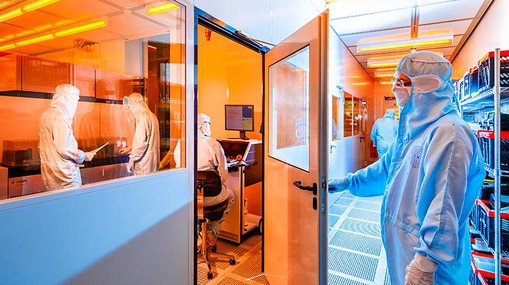
Center of MicroNanoTechnology
The CMi is a complex of clean rooms and processing equipment for the training and scientific experimentation devoted to the users of microtechnologies.
CMi – Center of MicroNanotechnology
Reservations
Organisation
Do you want to know more about CMi organisation?
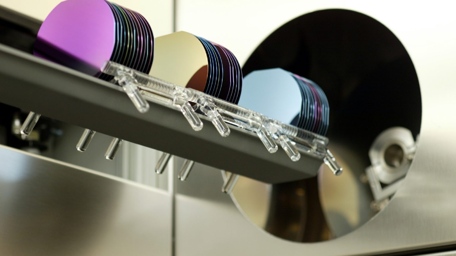
Equipment
CMi and its > 150 scientifics equipments
Process
Do you need help to execute some processes in CMi?
Our Mission:
- To provide basic and advanced training on processes and technologies.
- To offer access to the processing equipment available in the clean room.
- To gather, to practice and to provide the most advanced know-how in the microtechnology field.
- To cooperate with other academic institutions and research centers.
The CMi’s offer addresses:
- Education
- Scientific research, and
- Access to microfabrication processes
Picture of the month contest
To see images, please click here.

Picture of the month – Winners 2025
CMi Overview
Contact
Director of Operations
Dr Philippe Flückiger
E-mail: [email protected]
Tel: +41 (0) 21 693 66 95
Fax: +41 (0) 21 693 57 70
EPFL-CMi
BM 1.125 (BM Building) Station 17
CH-1015 Lausanne
GPS: 46.521144, 6.565360
GPS: 46.521125, 6.564963
Access map
Contact
Secretariat
Opening hours (People on site):
– Monday: 8:30 – 11:30 / 13:30 – 17:30
– Tuesday: 8:30 – 11:30 / 13:30 – 17:30
– Wednesday : 8:00 – 12:00
– Thursday : 8:30 – 11:30 / 13:30 – 17:30
– Friday : 8:30 – 11:30 / 13:30 – 17:30
– Monday: 8:30 – 11:30 / 13:30 – 17:30
– Tuesday: 8:30 – 11:30 / 13:30 – 17:30
– Wednesday : 8:00 – 12:00
– Thursday : 8:30 – 11:30 / 13:30 – 17:30
– Friday : 8:30 – 11:30 / 13:30 – 17:30
Tel: +41 (0) 21 693 57 33 Céline Cornaz
Tel: +41 (0) 21 693 56 97 Marie-Noëlle Verhar