Keywords: thin film silicon, amorphous silicon, microcrystalline silicon, micromorph, solar cells
Background
The “Thin Film Silicon Solar Cells on glass” group focuses on the development of high efficiency hydrogenated amorphous (a-Si:H) and microcrystalline (µc-Si:H) silicon single-junctions and multi-junctions solar cells in the superstrate configuration (p-i-n). The first µc-Si:H solar cells were pioneered at the PV-Lab in 1994. Microcrystalline silicon is of particular interest when combined with amorphous silicon in a solar cell tandem configuration, commonly called “micromorph”, as the different optical band gaps of these materials allow for the active conversion of a larger part of the solar spectrum. In such combination, a top a-Si:H cell absorbs light with wavelengths up to 800 nm while the µc-Si:H bottom cell can absorb light in the near infrared region, allowing for larger attainable conversion efficiencies. This “micromorph” serially connected tandem cell was first introduced at the PV-Lab in the mid 1990s, and since then, an increasing number of research institutes and companies have adopted this concept.
 |
 |
| Figure 1. SEM image (left) and schematic (right) of the cross section of a micromorph solar cell in the superstrate configuration. From bottom to top: glass – LPCVD textured ZnO – thin a-Si:H top cell (250 nm) – thin ZnO based intermediate reflector (200 nm) – 1.5 μm thick μc-Si:H bottom cell and back contact in LPCVD ZnO. | |
Microcrystalline silicon is a complex material that exhibits a wide range of possible microstructures depending on both the deposition conditions and substrate material. Many efforts have been laid in the past years in understanding the growth mechanisms of this material and the relationship between microstructure and solar cell efficiency. On the other hand, the amorphous nature and the metastable properties of hydrogenated amorphous silicon material also lead to different controversial issues remaining discussed, so that research remains active in this domain too. Finally, in order to achieve high efficiency with thin films of silicon, a high light confinement is fundamental and advanced cell designs integrating textured front-electrodes obtained via LPCVD deposition of ZnO or via the nano-imprinting fabrication of transparent nanostructures covered by highly transparent conductive oxides are developed, together with advanced solar cell designs allowing for high electrical properties on such rough substrates.
The main research areas of the group are as follows:
- Increasing thin film silicon solar cells efficiency by:
- Characterizing and improving the material quality (by modifying e.g. deposition processes) of microcrystalline silicon deposited in small-area laboratory PECVD systems and in semi-large area industrial PECVD systems.
- Improving the stability of a-Si:H solar cells to achieve larger stabilized efficiencies: protocrystalline materials and low deposition rate material to reduce the material degradation, or reduction of the impact onto the cell performance of the Staebler-Wronski effect.
- Implementing and assessing the light trapping potential in single to multi-junctions solar cells of new morphologies. Developments of novel concepts and materials to realize textured front electrode and substrate.
- Developing advanced concepts for optical confinement in the multi-junctions solar cells
- Improving the cell design to retain high electrical properties for cells deposited on highly textured substrates
- Testing different multi-junctions combinations and in that respect developing high-gap and low-gap materials
- Improving the solar cell design to ensure reduced cost of ownership for thin film silicon solar modules. One of the focus is for example on the development of high quality high deposition rate µc-Si:H material to decrease deposition time and hence production costs (strong collaboration with industries).
- Developing a better understanding of the relationship between plasma conditions, material quality and solar cell efficiency (in collaboration with the plasma group).
- Developing and implementing material and solar cell and modules characterization techniques
Research highlights
In the last years, notable progress in the understanding of the growth of microcrystalline silicon could be realized, and particularly the link between the material microstructure for different front contact morphology and the resulting solar cell efficiency. It could thus be demonstrated that unoptimized front contact morphology can lead locally to low-quality material regions (cracks) in the material. Such cracks consist in zones of porous material that are active in the mechanisms of post-oxidation of solar cells. This effect was highlighted by merging Scanning Electron Microscopy (SEM) (on cross-sections) and nano-SIMS (Secondary Ion Mass Spectroscopy) measurements, where a difference of oxygen concentration is clearly observed between dense material and cracks, see Figure 2 below:
 |
 |
| Figure 2. (Left) SEM on solar cell cross-section: μc-Si:H between front and back Zinc Oxide (ZnO). Cracks appear as dark lines. (Right) Mapping of oxygen concentration obtained by nano-SIMS method on a polished device cross-section. Pictures by M. Python et al published in Progress in Photovoltaics, 2010 | |
By combining improved front contact morphology and improved plasma processes, very high efficiencies could be achieved for single-junction and tandem solar cells. 9.9% could thus be achieved for single-junction microcrystalline silicon solar cell, which is among the best laboratories results (2006, presented at the 4th WCPEC conference).
In the case of micromorph tandems, the biggest challenge is to get a high current while maintaining a thin top cell: for this, intermediate reflector layers were introduced between the a-SI:H and µc-Si:H cells, realized either with LP-CVD ZnO or by in-situ deposited multi-phase material integrating silicon rich phases in a silicon oxide matrix. Very high currents up to 14.8 mA/cm2 in a 250 nm a-Si:H top cell of a micromorph could be demonstrated thanks to the use of a front ZnO layer allowing for large angle diffusion (2009, presented at the 24th EU PVSEC conference). The implementation of front contacts, design schemes and materials from both small-area and large-area deposition systems all developed in the laboratory allow the development of stable micromorph solar cells with stabilized efficiencies of 11.5 % (2010, presented at the 25th EU PVSEC conference), which is very close to the 11.7% world record of Kaneka. These different developments allowing for increasing the potential of thin film silicon technologies are and have been realized in the frame of different nationally funded and European funded projects.
 |
 |
| Figure 3. Measured characteristics of a 1.06 cm2 micromorph solar cell developed with a 240 nm a-Si:H top cell, 80 nm intermediate reflector and 2.8 µm thick bottom µC-Si:H cell, and light soaked for 1000 hours at 50 degrees and under an equivalent 1000 W/m2 AM1.5G illumination. (Left) External quantum efficiency demonstrating a high matched current of 13.3 mA/cm2, after LID. (Right) I-V characteristics after LID. | |
Our group works also in very close collaboration with many PV industries in the frame of different research mandates, one of the principal goal being here is to reduce the production costs of micromorph solar cells. Indeed, deposition time of the µc-Si:H bottom cell may easily reach up to 4 to 8 times that of the top a-Si:H, limiting throughput, while efficiency improvements do also have a direct impact onto the solar module cost of ownership (CoO). Strong developments are and were thus pursued in order to increase the efficiency, deposition rate and decrease the overall CoO.
 |
 |
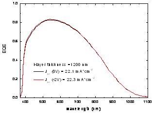
| Figure 4. Measured characteristics of a 0.25 cm2 1.2 µm thick microcrystalline solar cell developed at a deposition rate of 1 nm/s for the intrinsic-layer, in a semi-large area PECVD system (KAI-M). (Left) External quantum. (Right) I-V characteristics. (2010, presented at the MRS San Francisco) | |
Within the next years, the group will further investigate the different topics mentioned above, with focus on:
- Optimizing the c-Si:H deposition processes and material quality, as well as the cell design to achieve higher efficiencies on rough substrates
- Improving the a-Si:H material stability
- Increasing the efficiency of high rate c-Si:H material
- Modeling the relationship between internal plasma characteristics, process parameters and material quality
- Define the relative impacts of free carrier absorption, haze and angular diffusion fraction of TCOs onto the solar cell short circuit current density
- Developing advanced solar cell concepts for optimum light confinement and for improved efficiencies
Key publication
| [1] | M. Python, D. Dominé, T. Söderström, F. Meillaud, C. Ballif, Microcrystalline silicon solar cells: effect of substrate temperature on cracks and their role in post-oxidation, Progress in Photovoltaics: Research and Applications (2010) |
| [2] | G. Parascandolo, R. Bartlome, G. Bugnon, T. Söderström, B. Strahm, A. Feltrin and C. Ballif, Impact of secondary gas-phase reactions on microcrystalline silicon solar cells deposited at high rate, Applied Physics Letters 96 (23) (2010), 233508 |
| [3] | G. Bugnon, A. Feltrin, F. Meillaud, J. Bailat, and C. Ballif, Influence of pressure and silane depletion on microcrystalline silicon material quality and solar cell performance, Journal of Applied Physics 105 (2009), 064507 |
| [4] | M. Despeisse, G. Bugnon, A. Feltrin, M. Stueckelberger, P. Cuony, F. Meillaud, A. Billet, and C. Ballif, Resistive interlayer for improved performance of thin film silicon solar cells on highly textured substrate, Applied Physics Letters 96 (2010), 073507 |
| [5] | C. Battaglia, K. Söderström, J. Escarré, F-J. Haug, D. Dominé, P. Cuony, M. Boccard, G. Bugnon, C. Denizot, M. Despeisse, A. Feltrin and C. Ballif, Efficient light management scheme for thin film silicon solar cells via transparent random nanostructures fabricated by nanoimprinting, Applied Physics Letters, Vol 96, pp. 213504-, 2010 |