Nanoscale electronics and structures
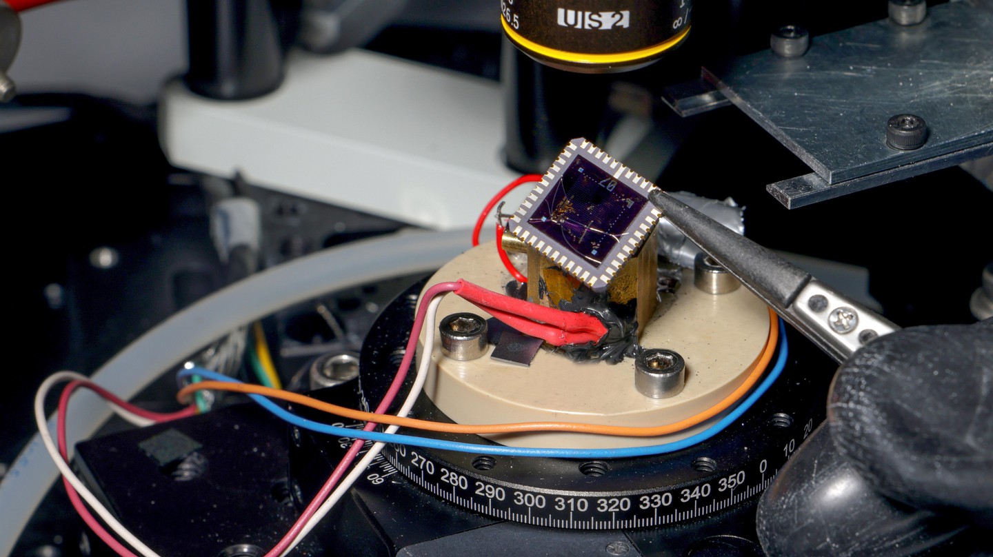
We are working on nanoelectronics based on two-dimensional materials such as monolayers of transition metal dichalcogenides (MoS2, WSe2, MoSe2,..). In 2010 we demonstrated a transistor based on a single, two-dimensional layer of semiconducting MoS2. This showed for the first time that high-quality devices can be made using this class of materials, opening the way to studying their fundamental properties and practical applications.MoS2 and related materials are now one of top ten hottest areas in physics.We investigate electrical properties, fundamental physics and practical applications of 2D materials in a vertically integrated approach. We grow 2D materials, incorporate them into devices in the EPFL class 100 1500 m2 cleanroom, perform electrical, optical and nanomechanical characterization using our fully equipped electronics and optics labs.