 ACI – CAO
A Footprint Catalogue can be found under: Footprint Catalogue (pdf)
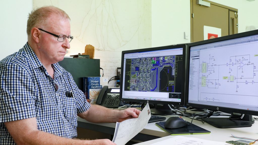
We are experts in PCB design with extensive experience in high speed digital, analog and RF for single, double, and high layer count boards. Whether your project entails high speed constraint-driven requirements or basic I/O, our staff has the expertise to deliver a comprehensive design package that is well-managed, on-time, and right the first time.
Capabilities and Services offered:
- Board layout from a customer supplied schematic diagram
- Schematic capture (small projects only)
- Telesis import from Altium schematic
- Chip on board
- Controlled impedance
- Multi-layer boards, mixed-signal, high speed rules, differential pairs
- Routing per trace/space, keep-out, and clearance rules specified by customer
- Surface mount or through hole designs
- Unusual PCB shapes with DXF files
Deliverables offered:
- Assembly drawings, fabrication drawings all in on pdf file
- e-puck.org (pdf)
- LinoSPAD (pdf)
- Bill of materials and pick and place files generation
- Board artwork, SMT solder paste stencil artwork, CAM data generation
If you have any questions or inquiries, please contact Mr. Jean-Marie Barblan (Tél. 377 68)