Silicon-based heterojunction solar cells
| Group members: | M. Boccard, L. Antognini, J. Cattin, J. Dréon, O. Dupré, A. Fioretti, J. Haschke, R. Monnard, E. Rucavado, S. Zhong |
| Running projects: | European Commission (EU), EuroTech University Alliance, Qatar Fundation (QEERI), Office fédéral de l’énergie (OFEN), Fonds national suisse (FNS), Swiss Commission for Technology and Innovation (CTI). |
Keywords: Photovoltaics, solar cells, crystalline silicon, amorphous silicon, PECVD, carrier-selective contacts, metal-oxides, energy yield, heterojunction, high-efficiency.
Background
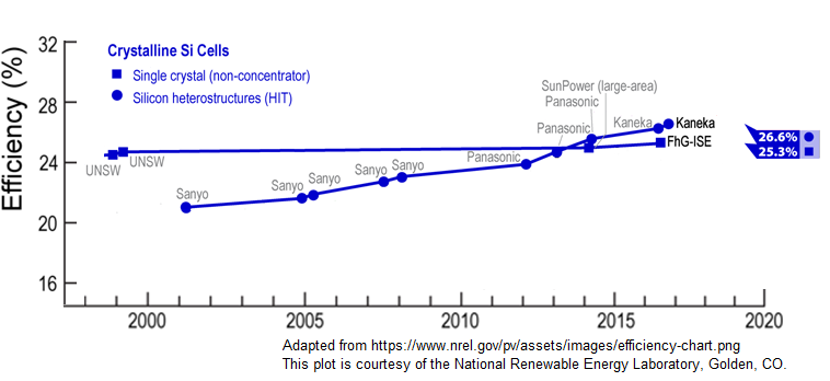
Photovoltaics (PV) energy is on the edge of becoming one of the main global source of energy, and crystalline silicon has been dominating the market with no sign of change in the near future. Silicon-based heterojunction solar cells (Si-HJT) are a hot topic within crystalline silicon photovoltaic as it allows for solar cells with record-efficiency energy conversion up to 26.6% (Fig. 1, see also Yoshikawa et al., Nature Energy 2, 2017). The key point of Si-HJT is the displacement of highly recombination-active contacts from the crystalline surface by insertion of a film with wide bandgap. To reach the full device potential, the hetero-interface state density should be minimal. Practically, hydrogenated amorphous silicon (a-Si:H) films of only a few nanometers of thickness are appealing candidates for this: Their bandgap is wider than that of c-Si and, when intrinsic, such films can reduce the c-Si surface state density by hydrogenation. In addition, these films can be doped relatively easily, either n- or p-type, allowing for the (lithography-free) fabrication of contacts with record-low values for the saturation-current density. Impressive large-area (> 100 cm2) energy-conversion efficiencies (~25%) have been reported by several companies (Tagushi et al., IEEE JPV 4, 2014, Adachi et al. APL 104, 2015 …).
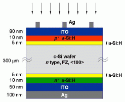
A sketch and band diagram of a typical heterojunction solar cell are given in Figure 2. The basic device features on the front (illumination) side successively an intrinsic a-Si:H passivation layer and a p-doped amorphous silicon emitter both deposited by plasma enhanced chemical vapor deposition (PECVD). On top of the silicon layers, an antireflective transparent conductive oxide (TCO) is deposited by physical vapor deposition (PVD) and the charge collection is made by a screen-printed metallic contacting grid. On the back side, an electron collecting stack is used, and it is composed of an intrinsic a-Si:H passivation layer, a doped n-type amorphous silicon (both deposited by PECVD), a TCO layer and a metallic contacting layer (deposited by PVD).
 |
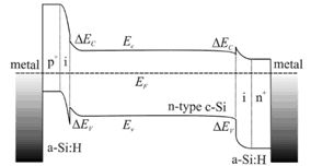 |
Figure 2: Left: Schematic diagram of a heterojunction solar cell (not to scale). Right: Electronic band diagram in dark at equilibrium of a heterojunction solar cell (not to scale).
Figure 3 displays the main topics of research currently pursued in the group. This goes from fundamentals of passivation mechanism, through the development of alternative contact schemes to extract the negative (electrons) and positive (holes) electrical charges, to the development of innovative device architectures and the study of the impact of operating conditions on the energy yield of photovoltaic modules.
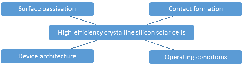
Figure 3: Active research topics around Silicon-based heterojunction solar cells.
Recent advances in large-scale production of high-purity silicon made very-high-quality silicon wafer readily available for mass production. The low defect density in such wafers makes efficiencies over 25% achievable for proper device architecture. The first challenge to make such high-efficiency device is to ensure that the surface of the wafer does not present electronically active defects. Such surface passivation can be achieved in various ways, the most widely investigated in PV-Lab being the use of plasma-deposited hydrogenated amorphous silicon (a-Si:H). This proves to be one of the most efficient layer to provide extremely good passivation, allowing very large carrier lifetimes in silicon wafers, as well as record-high efficiencies. The phenomena behind surface passivation from a-Si:H (and its oxide and carbide alloys), the role of hydrogen, the effect of heating or light-illumination are fascinating scientific interrogations which make this field still very active [Kobayashi2016].
The second challenge when building a highly-efficient solar cell from a high-quality silicon wafer is the selective collection of positive and negative charges at two spatially separated terminals. Such selective collection relies on semi-permeable electronic membranes, offering a low-resistance electrical connection for one type of charges (e.g. electrons) while blocking with minimal leakage the other type (holes). The use of doped amorphous silicon layers (p-type and n-type a-Si:H) prove to be an extremely efficient way of providing such selectivity with world-record efficiencies obtained using such contacts by several laboratories and companies [DeWolf2012]. Those films present several limitations, including parasitic absorption of light and non-ideal selectivity (with notably a non-negligible resistance to charge extraction and low lateral conduction). Unravelling the fundamental properties required for an ideal selective contact (involving material but also interface properties) is key for developing more efficient devices based on simpler processes. Applying novel suitable materials as carrier-selective contacts is a very active topic to this end and designing and fabricating suitable materials is a strong focus of the group.
Dopant-free solar cells: While a long-lived idea that a photovoltaic device required doped contacts of opposite polarities to be efficient, a recent understanding of the physics of solar cells suggested that it was not the case: Several contact architectures can theoretically provide similarly efficient devices. The experimental demonstration of a high-efficiency yet entirely dopant-free crystalline silicon cell — using slightly sub-stoichiometric MoO3 and LiF as hole- and electron-selective contacts — opens the road towards entirely new device architecture, with much simplified processes and extremely simple designs [Bullock2016].
Interdigitated back contacted (IBC) solar cells: To extract the electrical charges from a silicon solar cell, metal contacts are required. Whereas in the traditional-architecture solar cells negative (electrons) and positive (holes) charges are collected on each side of the wafer, the IBC design collects both charge types on the rear of the wafer. This allows to place all the metal required to extract these charges on the rear of the wafer, thus preventing shadowing and allowing a higher current to be generated. While simple in principle, such approach presents many scientific and technological challenges [Tomasi2017].
Small-area devices: Whereas record cells for most photovoltaic technologies are obtained on small-area devices (1 cm2 or below), recent record efficiencies for wafer-based silicon devices were obtained on much larger area > 100 cm2. The large diffusion length of photogenerated carriers in silicon (typically of millimeter scale) makes edge recombination a particular issue, and the fabrication of small devices challenging. A better understanding of area-related losses and development of edge passivation could allow efficient small-area devices to be made relaxing needs in terms of metallization.
Common optimization of solar cells is made to reach highest performances under standard test conditions (25 °C, 1000 W/m2, AM1.5 spectrum). Such conditions are not representative of the ones experienced in the field during operation. In particular, modules installed in hot and sunny climates experience a high irradiance level but also a high operating temperature which is detrimental to their energy output. High operating temperatures can however be beneficial in particular cases to overcome thermionic barriers and improve charge transport. Tailored optimization for specific climatic conditions can provide several percent annual energy gain over standard approaches. It was also shown that resistance losses due to cell interconnection impact not only the module efficiency but also the temperature coefficient of modules, highlighting the stronger need for low-resistance interconnection in hot climates [Haschke2017].
Recent publications:
| [Tomasi2017] | A. Tomasi, B. Paviet-Salomon, Q. Jeangros, J. Haschke, G. Christmann, L. Barraud, A. Descoeudres, J. P. Seif, S. Nicolay, M. Despeisse, S. De Wolf, and C. Ballif “Simple processing of back-contacted silicon heterojunction solar cells using selective-area crystalline growth,” Nature Energy 2, 17062, 2017 (Doi:10.1038/nenergy.2017.62) |
| [Haschke2017] | J. Haschke, J. P: Seif, Y. Riesen, A. Tomasi, J. Cattin, L. Tous, …, and C. Ballif, “The Impact of Silicon Solar Cell Architecture and Cell Interconnection on Energy Yield in Hot & Sunny Climates.” Energy & Environmental Science, 2017 (DOI:10.1039/C7EE00286F) |
| [Kobayashi2016] | E. Kobayashi, S. De Wolf, J. Levrat, G. Christmann, A. Descoeudres, S. Nicolay, M. Despeisse, Y. Watabe, and C. Ballif, “Light-induced performance increase of silicon heterojunction solar cells.” Appl. Phys. Lett. 109, no. 15, 2016 (DOI: http://dx.doi.org/10.1063/1.4964835) |
| [Seif2016] | J. P. Seif, A. Descoeudreas, G. Nogay, S. Hänni, S. Martin de Nicolas, N. Holm, J. Geissbühler, A. Hessler-Wyser, M. Duchamp, R. E. Dunin-Borkowski, M. Ledinsky, S. De Wolf, and C. Ballif, ” Strategies for doped nanocrystalline silicon integration in silicon heterojunction solar cells.” IEEE J. Photovoltaics, Volume 6, no.5, 2016 |
| [Bullock2016] | J. Bullock, M. Hettick, J. Geissbühler, A. J. Ong, T. Allen, C. M. Sutter-Fella, T. Chen, H. Ota, E. W. Schaler, S. De Wolf, C. Ballif, A. Cuevas, and A. Javey, “Efficient silicon solar cells with dopant-free asymmetric heterocontacts.” Nature Energy 1, 15031, 2016 (DOI:10.1038/nenergy.2015.31) |
| [Tomasi2016] | A. Tomasi, F. Sahli, J. P. Seif, L. Fanni, S. Martin de Nicolas Agut, J. Geissbühler, B. Paviet-Salomon, S. Nicolay, L. Barraud, B. Niesen, S. De Wolf, and C. Ballif, “Transparent electrodes in silicon heterojunction solar cells: Influence on contact passivation,” IEEE J. Photovoltaics, Volume 6, no.1, 2016 (DOI: 10.1109/JPHOTOV.2015.2484962) |
| [Geissbühler2015] | J. Geissbühler, J. Werner, S. Martin de Nicolas, L. Barraud, A. Hessler-Wyser, M. Despeisse, S. Nicolay, A. Tomasi, B. Niesen, S. De Wolf, and C. Ballif, “22.5% efficient silicon heterojunction solar cell with molybdenum oxide hole collector.” , Appl. Phys. Lett. 107, no. 8, 2015 (DOI: http://dx.doi.org/10.1063/1.4928747) |
| [Seif2015] | J. P. Seif, G. Krishnamani, B. Demaurex, Christophe Ballif, and Stefaan De Wolf. “Amorphous/crystalline silicon interface passivation: ambient-temperature dependence and implications for solar cell performance.” IEEE J. Photovoltaics, Volume 5, no.3, pages 718-724, 2015 (DOI: 10.1109/JPHOTOV.2015.2397602 ) |
| [DeWolf2012] | S. De Wolf , A. Descoeudres, Z. C. Holman, C. Ballif, High-efficiency Silicon Heterojunction Solar Cells: A Review, Green, Volume 2, Issue 1, Pages 7–24, 2012 |