Ultraviolet (UV) wavelengths have been of particular interest in space applications for their importance in the study of planetary bodies and their atmospheres [1,2]. The UV spectrum provides essential information of various elements and compounds, helping us better understand the nature and habitability of the planetary bodies. All of these are not possible without high-performance photodetectors, with photon counting capability necessary for faint object detection. Addressing these challenges, NASA’s Jet Propulsion Laboratory (JPL) in California developed Gallium nitride (GaN) avalanche photodiodes (APDs) for UV imaging, particularly useful because of their wide bandgap and tailorable out-of-band cutoff from 3.4 eV to 6.2 eV. Reverse-biased typically at high voltages (≈80 V), the GaN APDs generate currents on the order of hundreds of picoamperes in proportional-mode (as shown in Figure 1), while avalanching to more than a few microamperes beyond the breakdown voltage. Challenges exist however for practical utilization, mainly because of the lack of integration to an imaging system. This limitation, thus, imposes the fundamental need to have an appropriate readout solution [1,2].
In this work, we have been collaborating with JPL to develop a suitable readout solution for their GaN APDs operating in proportional mode. In the first version, we implemented and tested a CMOS front-end circuit, comprising of a linear array of 1×8 capacitive transimpedance amplifiers (CTIAs), implemented in a 0.35µm high voltage CMOS technology. The readout offers a conversion gain of 0.43 µV/e−, obtaining avalanche gains up to 103 (Figure 2). The work done so far is a proof-of-concept demonstrating the feasibility of our approach of combining GaN APDs with CMOS circuits. This work in future can lead towards a 3D-integrated chip where APDs can be stacked on top of the custom CMOS circuit. Furthermore, based on the compatibility of the detector substrate with silicon, the hybrid concept can allow easy porting of our CMOS circuits to any kind of photodetector, including the GaN-based detectors discussed here [2]. Figure 3b shows the conceptual representation of such a possibility.
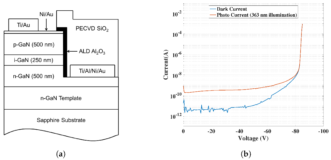
GaN APDs developed at JPL- device geometry (a) and I-V curve (b)
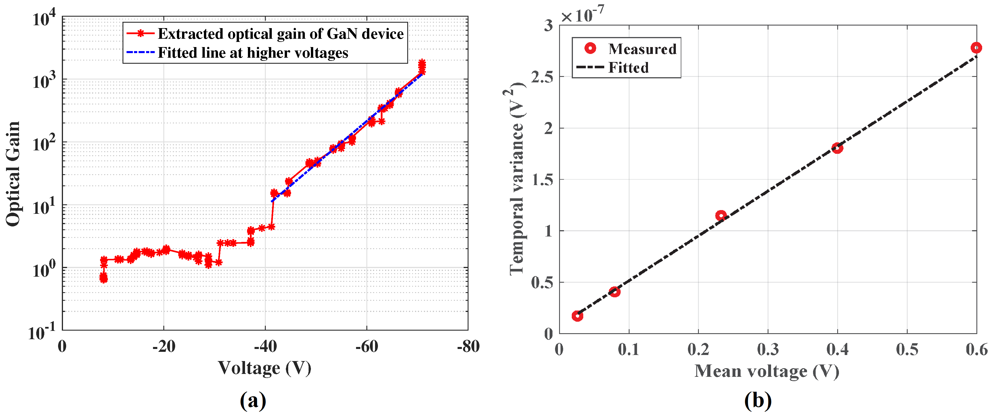
GaN sensor measurement- Optical gain measured (a) and temporal variance versus mean output voltage; slope of the line gives the conversion gain- 0.43 µV/e–
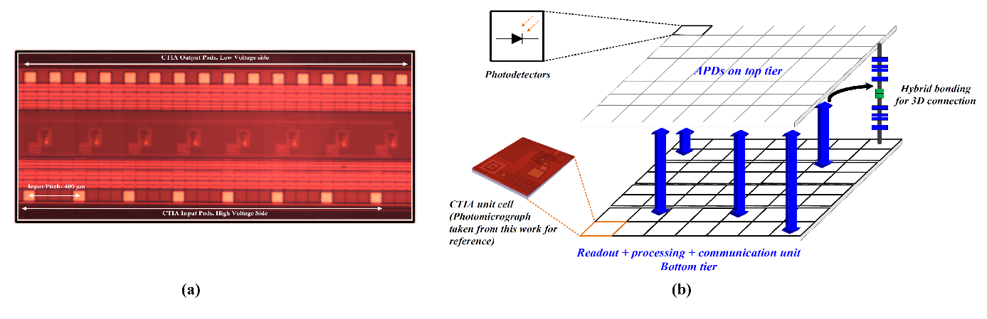
Chip micrograph of the readout showing 8 units of CTIAs (a) and conceptual representation of 3D stacking concept (b)
Relevant publications
S. Nikzad; M. Hoenk; A. Jewell; J. Hennessy; A. Carver et al. : Single Photon Counting UV Solar-Blind Detectors Using Silicon and III-Nitride Materials; Sensors. 2016-06-21.
P. Padmanabhan; B. Hancock; S. Nikzad; L. Bell; K. Kroep et al. : A Hybrid Readout Solution for GaN-Based Detectors Using CMOS Technology; Sensors. 2018-02-03.
Collaboration
Jet Propulsion Laboratory, California